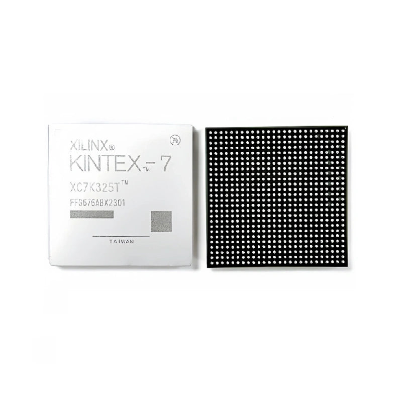
XC7K325T-2FFG676I - High-Speed FPGA Chip with 326K Logic Cells
Couldn't load pickup availability
Have questions about this product? Our team is here to help — just reach out on WhatsApp.
💬 Contact Us on WhatsAppAbout the Product
XC7K325T-2FFG676I Kintex-7 FPGA – 326K Logic Cells for High-Performance Applications
The XC7K325T-2FFG676I is a Xilinx Kintex-7 FPGA with 326,080 logic cells, 15.6Mb embedded Block RAM, up to 400 I/O ports and 16× 12.5Gb/s transceivers in a 676-FCBGA package. It supports DDR3/DDR4 memory at 1,866Mb/s, PCIe Gen3 and 10G Ethernet. Operating voltage 0.97–1.03V, temperature range -40°C to +100°C. Used in mining overclocking boards, 5G base stations, radar systems, industrial automation and AI acceleration.
Why Kintex-7 in Mining
The XC7K325T is the FPGA at the heart of advanced Antminer overclocking boards like the KINTEX-7 based S19/T19 overclock controller. Its 326K logic cells provide enough configurable fabric to implement custom hashboard voltage/frequency control logic that outperforms stock firmware overclocking — delivering 18–30% hash rate improvements with tighter chip-level management.
Applications
Beyond mining, the XC7K325T serves in beamforming for 5G infrastructure, real-time image processing, defence radar systems, telecommunications switching and high-performance computing environments where configurable, high-bandwidth processing is required.
XC7K325T FPGA Specifications
| Parameter | Value |
|---|---|
| Family | Kintex-7 |
| Logic Cells | 326,080 |
| Block RAM | 15.6Mb |
| I/O Ports | 400 max |
| Transceivers | 16× 12.5Gb/s |
| Package | 676-FCBGA |
| Vcore | 0.97–1.03V |
| Temperature | -40°C to +100°C |
| Condition | New |
Related FPGA & Logic Chips
Sourcing FPGAs for overclocking or industrial projects? Contact us at contact@lys-sz.com for availability and pricing. Worldwide shipping from our Shenzhen warehouse.
Buying in bulk for a mining farm or repair shop?
Get dedicated B2B pricing on this part and across our full catalog — quote response within 24 hours, payment by T/T USD bank wire, and DDP delivery available for US & EU customers (and other lanes on request).