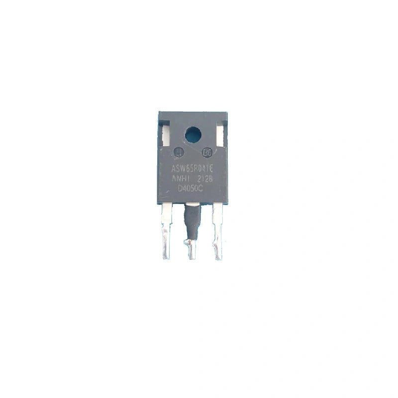
ASW65R041E Low Drain-Source On-Resistance N-Channel MOSFET
Couldn't load pickup availability
Have questions about this product? Our team is here to help — just reach out on WhatsApp.
💬 Contact Us on WhatsAppAbout the Product
Enhance Power Efficiency with the ASW65R041E N-Channel MOSFET
The ASW65R041E is a high-quality N-Channel MOSFET designed to deliver efficient power control and reliable performance. With its low drain-source on-resistance and easy gate switching control, this MOSFET is ideal for a wide range of applications, including soft switching Boost PFC, HB or AHB, LLC bridge, full bridge topologies, and phase-shifting bridge (ZVS) configurations.
Optimized Gate Switching and Versatile Applications for Power Systems
The ASW65R041E operates in enhancement mode, with a threshold voltage (Vth) ranging from 2.8V to 2V. This mode enables ease of use and flexibility in various power system designs.
ASW65R041E Technical Features:
| Feature | Description |
|---|---|
| Low Drain-Source On-Resistance | Ultra-low RDS(ON) for minimized power loss |
| Easy Gate Switching Control | Simplified control of gate switching for precise operation |
| Enhancement Mode | Operates in enhancement mode for versatility in power systems |
ASW65R041E Parameters:
- VDsTjmax (Maximum Drain-Source Voltage at Maximum Junction Temperature): 700V
- RDs(on),max (Maximum Drain-Source On-Resistance): 41mΩ
- Qg,typ (Typical Total Gate Charge): 133.5nC
- ID.pulse (Pulsed Drain Current): 240A

Buying in bulk for a mining farm or repair shop?
Get dedicated B2B pricing on this part and across our full catalog — quote response within 24 hours, payment by T/T USD bank wire, and DDP delivery available for US & EU customers (and other lanes on request).