Antminer T21 & S21 Hashboard Repair Guide & Components List (2026 Update)
The Antminer S21 and T21 are Bitmain's current-generation 5nm flagships — built around the BM1368 ASIC chip family and the BHB68XXX hashboard architecture, delivering ~200 TH/s at 17.5 J/TH on the standard S21. Two years after their late-2024 launch, both models are the highest-volume miners entering secondary-market repair, and the components inventory required to keep them producing is largely shared between the two platforms. This guide covers the BM1368 chip variants, the unique 12-domain × 9-chip topology, the level-shifter additions that distinguish the BHB68XXX from older Antminer architectures, and the full components list with direct sourcing links for every part.
Why T21 & S21 Hashboard Repair Matters in 2026
The S21 platform is the most-deployed efficient miner in current post-halving operations. With ~$2-3/TH secondary market pricing on used units and full hashboard replacements pricing at multiples of component-level repair cost, chip-level and component-level repair is the most economical way to keep production going. The T21 shares the same hashboard architecture as the S21, meaning a single repair-bench inventory covers both platforms.
Antminer S21 & T21 Hashboard Architecture at a Glance
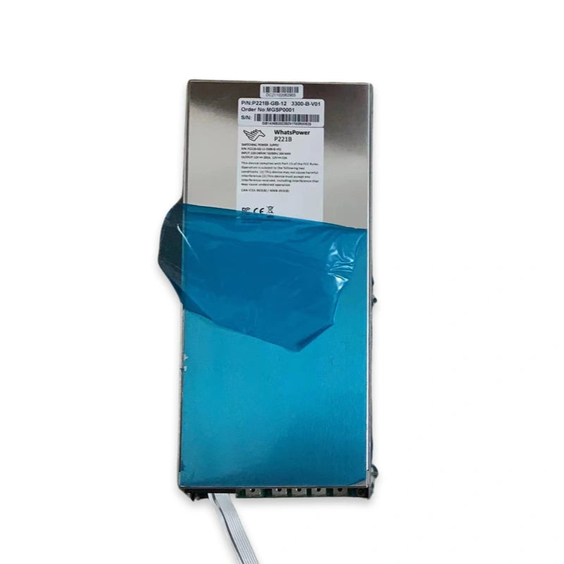
The S21 and T21 hashboards share the same BHB68XXX board family — built around the BM1368 ASIC chip generation. Multiple silicon revisions ship across production: BM1368PB, BM1368PA, BM1368PV, BM1368PM, and BM1368AA — all used as replacement chips across the S21, T21, S21 IMM (immersion), and S21 Hydro variants. The chips are LGA-packaged (6 mm × 8 mm footprint), which makes the stencil tool requirement specific to this generation.
Each BHB68XXX hashboard carries 108 BM1368 chips, organised as 12 voltage domains of 9 chips in series (silkscreen sequence BM1 through BM108). The nominal domain operating voltage is approximately 1.2V at rest. A complete miner uses 3 hashboards per chassis. The two platforms diverge only at the PSU choice:
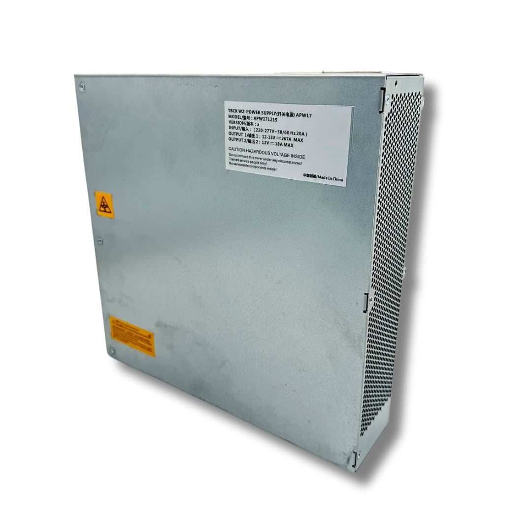
- S21: APW171215a PSU (12V-15V, V1.3)
- T21: APW11A1216-1a PSU (12V-16V, V1.1)
The control board ecosystem matches the rest of the Antminer line (AMLogic / 7Z007 variants) with the standard U1 FBGA main IC carrying the OTP one-time-programmable function.
Per-domain power topology
The BHB68XXX power architecture differs between standard and high-voltage domains:
- Domains 1 to 10 (standard): each domain has 3 LDOs — one outputting 1.2V (VDDIO), two outputting 0.8V (chip core). The chips draw their rails directly from these LDOs.
- Domains 11 and 12 (high-voltage): each uses two MP2019 LDOs at positions U166 and U200 to first generate 2V, which then supplies the local 1.2V / 0.8V LDOs (U165/U167 powered by U166; U199/U201 powered by U200). A failed MP2019 takes the entire high-voltage domain offline.
What changed from earlier Bitmain hashboards
The BHB68XXX architecture removed and added several components compared to the BM1362 (S19j family) and BM1398 (S19 family) generations:
- Removed: the PIC microcontroller and the dedicated MOS circuit from the chip-side stage. This simplifies the diagnostic tree but removes some intermediate fault-isolation points.
- Added: 11 operational amplifiers (level shifters) — one between each domain pair from domain 2 to domain 12. These perform signal addition operations on the chip data path. Level shifters 0 to 9 derive power from the 5-domain stack voltage (approximately 6V); level shifters 10 and 11 are powered by U118 (VDD_LDO sourced from the 19V boost circuit). When PT1 or PT3 testing reports a fault at the 2-domain handover position, the op-amps are the first place to check.
BHB68XXX boost circuit and rail topology
The boost stage takes VDD_IN through chip U206 and steps it up to approximately 25V. This boosted rail feeds the U118 supply that powers level shifters 10 and 11 plus the high-voltage domains' MP2019 chain. A failed boost stage drops the upper level shifters and the high-voltage domains simultaneously, presenting as a fault concentrated at the back-half of the chain scan.
BHB68XXX signal directions — critical for chain-fault diagnosis
- CLK: generated by the Y1 25 MHz crystal oscillator, flows forward from BM1 to BM108. Operating voltage approximately 0.58-0.6V.
- TX (CI / CO): enters at pin 7 of the IO interface at 3.3V, passes through level-shifting IC U1, flows forward from BM1 to BM108. Operating voltage approximately 1.1V.
- RX (RI / RO): reverse direction — flows from BM108 back to BM1, returns to pin 8 of the signal cable through U2, then to the control board. Operating voltage approximately 1.1V.
- BO (BI / BO): flows forward from BM1 to BM108.
- RST: enters at pin 3 of the IO interface, passes through R1020, flows forward from BM1 to BM108. Operating voltage approximately 1.2V.
The chassis chain numbering: Chain0 = board 1 (middle position varies by chassis), Chain1 = middle board, Chain2 = board adjacent to the PSU.
Most Common S21 & T21 Hashboard Failure Modes
- 0 chips detected at boot — walk the power chain: VDD_IN present → boost output (25V) → per-domain LDO 1.2V and 0.8V → chip signal voltages (CLK / CI / RST / RO / BI in their respective ranges).
- EEPROM NG on test fixture LCD — check U6 GT24C02A EEPROM soldering and the ribbon cable connection.
- Sensor NG (sensor=0 or sensor=1) — corresponds to U5 (inlet) or U7 (outlet) S75 temperature sensor. Check the sensor IC, adjacent SMD passives, and the 3.3V supply at J213.
- INIT NG TEMP — abnormal inlet/outlet temperature; check U4, U5, U7 and their nearby passives.
- Fault at the 2-domain handover position — almost always an op-amp / level-shifter issue. Check the 11 added level shifters starting from domain 2.
- 3.3V short circuit — can burn U5 and U7 (sensors) via cascade. Always measure 3.3V impedance to ground before powering up. If shorted, identify and disconnect the offending component to clear the short before reapplying power.
- Pattern NG with low nonce response — chip die damage, virtual soldering, or bridging. Use the BM1368 LGA stencil for clean reflow.
- "find x asic" with x < 108 in the whole-machine log — incomplete chain detection. Use PT1 to isolate the missing position via binary search.
Critical Components — Function & Failure Behaviour
ASIC Hash Engine (BM1368 family)
The BM1368 family is the hash engine of the BHB68XXX hashboard. Five silicon revisions are in service: BM1368PB, BM1368PA, BM1368PV, BM1368PM, and BM1368AA — all cross-compatible across S21, T21, S21 IMM, and S21 Hydro hashboards. Each chip is LGA-packaged with a 6 mm × 8 mm footprint, requiring the dedicated BM1368 stencil for reballing. ESD damage during handling and sustained thermal stress from dried thermal paste are the most common failure causes.
Voltage Regulators (LDOs & high-voltage stage)
The hashboard uses BA1U / BA2X (0.8V) as the chip core LDO, VGML AAH6 (1.2V) as the VDDIO LDO, and MP2019 (1.8V / 2V high-voltage stage) for the domains 11/12 supplies at U166 and U200. The LM317MBSTT3G provides an adjustable 500 mA positive regulator for support stages. A failed LDO in domains 1-10 takes its local 9-chip group offline; a failed MP2019 in domains 11/12 cascades to take the whole high-voltage domain down.
Boost Regulator (SY7304DBC)
The SY7304DBC (VIDKB) current-mode boost regulator supports the boost stage. A failed boost stage drops the upper domain rails and level-shifter supplies simultaneously.
Level Shifters (Op-Amps) — Unique to BHB68XXX
The SGM8304 operational amplifier module handles the level-shift / signal-addition operations across domain handovers. The board carries 11 level shifters from domain 2 to domain 12. The SN74AUP1T34DCKR (U2E) handles the 3.3V-to-chip-side signalling at U1 and U2.
EEPROM (GT24C02A)
The GT24C02A (GT402A) EEPROM at U6 stores calibration and chain identification data. A corrupted EEPROM produces EEPROM NG on the test fixture LCD and blocks enumeration.
Temperature Sensor (S75)
Two S75 digital temperature sensors at positions U5 (inlet) and U7 (outlet) monitor hashboard temperature. A failed sensor produces missing or implausible readings — the sensor index in the serial log maps to U5 (sensor=0) or U7 (sensor=1). Always verify the 3.3V supply at J213 before replacing the sensor IC.
Protection Diodes
The SMBJ190A (PA) TVS diode and DSK24 Schottky diode handle on-board ESD clamping, freewheeling, and overvoltage protection.
Passive Components
The G337 2V tantalum, 330µF 30V SMD, and 47µF 50V SMD capacitors handle bulk decoupling. The 10µH HPC1050 inductor handles boost-stage energy storage. The 1R80 1206 SMD resistor serves as a current-sense element. Common spare passive inventory includes 0402 resistors (0R, 33Ω±1%, 10K) and 0402 capacitors (1µF, 22µF).
Antminer T21 & S21 Hashboard Repair Components List
The table below lists every component LYS Shenzhen stocks for T21 / S21 hashboard repair. Each entry links directly to the corresponding part page — contact us at contact@lys-sz.com for bulk pricing, for BM1368 chip variants not currently in stock, or for the 1R80 SMD 1206 resistor.
| Part Number | Component Type | Typical Position / Role |
|---|---|---|
| BM1368 PB / PA / PM / AA | ASIC hash engine | 5nm SHA-256, 108 per board across 12 domains × 9 chips (LGA 6×8 mm) |
| SMBJ190A (PA) | TVS diode | Transient overvoltage protection |
| GT24C02A (GT402A) | EEPROM | U6 — calibration / chain ID storage |
| BA1U / BA2X | LDO regulator | 0.8V chip core rail (per-domain) |
| S75 | Temperature sensor | U5 inlet + U7 outlet, 3.3V supply at J213 |
| SY7304DBC (VIDKB) | Boost regulator IC | Current-mode boost stage |
| DSK24 | Schottky diode | 2A / 40V freewheeling diode |
| 10µH (Inductor 100) | Inductor | HPC1050 SMD boost-stage energy storage |
| SGM8304 Module | Operational amplifier | 11 level shifters across domain 2-12 handovers |
| G337 2V | Tantalum capacitor | Low-ESR polymer KO-CAP, bulk decoupling |
| 330µF 30V SMD | Capacitor | Bulk filtering on power-delivery stage |
| 47µF 50V SMD | Capacitor | Local rail bulk capacitor |
| 1R80 SMD 1206 | Resistor | Current-sense / shunt — contact us for stock check |
| MP2019 (SOP8) | LDO regulator | 1.8V rail + 2V supply for high-voltage domains 11/12 at U166/U200 |
| VGML AAH6 | LDO regulator | 1.2V VDDIO supply (per-domain) |
| LM317MBSTT3G | Positive regulator | 500 mA adjustable output |
| SN74AUP1T34DCKR U2E | Voltage level translator | 3.3V to chip-side signalling at U1 / U2 |
Required Repair Tools & Consumables
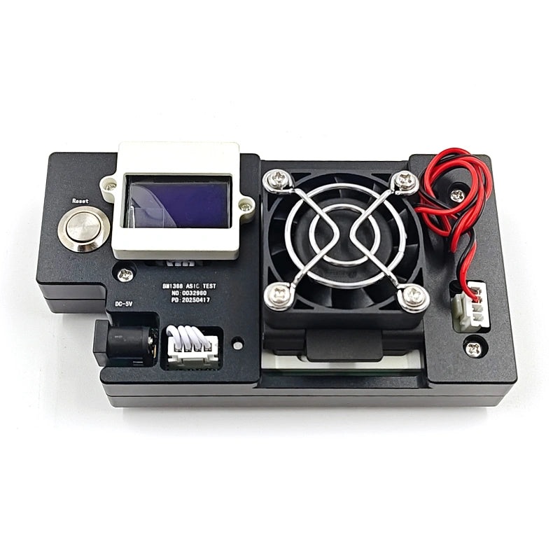
- Universal hashboard test fixture with LCD — supports PT1 (chip detect) and PT3 (sweep functional) on BHB68XXX. The 19-series fixture requires the B047 firmware flash for S21/T21 compatibility.
- BM1368 LGA 6×8 mm tin stencil — dedicated to the BM1368 chip footprint (the older BM1362 / BM1366 stencils do not match).
- Constant-temperature soldering iron set to 350–380°C with a pointed tip for SMT work.
- Hot-air rework station and BGA rework station for chip removal and placement.
- Solder paste M705 grade, no-clean flux, board washing fluid with anhydrous alcohol.
- Tin balls 0.4 mm diameter for chip ball reattach work.
- Multimeter (Fluke recommended) with welded steel probe needles and heat-shrink sleeves.
- Oscilloscope for signal-path verification.
- Thermal compound rated 5W/mK or higher — required for 24/7 mining loads.
- Common spare 0402 resistors (0R, 33Ω±1%, 10K) and 0402 capacitors (1µF, 22µF).
- 4 AWG copper wire (under 60 cm) for bench-power leads to the hashboard.
Diagnostic and Repair Workflow
- Power off and remove the suspect hashboard from the miner — never work on a powered board.
- Visual inspection — look for scorched components, lifted pads, PCB deformation, or impact damage.
- Identify the platform: S21 uses APW171215a, T21 uses APW11A1216-1a. Wrong-PSU bench setup will not deliver the right input voltage to the board.
- Impedance / short-circuit check on every voltage domain and the 3.3V rail before powering. A 3.3V short can burn U5/U7 sensors on power-up.
- Power-on the test fixture in the correct sequence: connect the negative copper supply lead first, then the positive copper lead, and finally plug in the signal cable. Reverse the sequence to disconnect.
- Run PT1 chip detection first, then PT3 sweep functional test once PT1 passes.
- If 0 chips reported, walk the power chain: VDD_IN → 25V boost output at U206 → per-domain LDO 1.2V and 0.8V → chip signal voltages (CLK ~0.6V, CI ~1.1V, RST ~1.2V).
- If sensor NG, check U5 and U7 plus the J213 3.3V supply and adjacent passives.
- If fault at domain handover position, check the 11 op-amp level shifters — this is a BHB68XXX-specific diagnostic point absent on older Antminer hashboards.
- Binary-search fault isolation for incomplete chip detection: short the 1.2V rail to the RO test point between candidate chip boundaries and re-run the chip-find program.
- For chip replacement: use the BM1368 LGA stencil to pre-tin the chip pins with M705 paste before placing on the PCBA.
- Re-test on the fixture twice — let the board cool to ambient between runs. Both runs must pass cleanly.
- Re-paste the heatsink with 5W/mK or higher thermal compound before reassembly. The BHB68XXX requires the large heatsink fully installed during PT3 functional testing.
- Reinstall and monitor for 24 hours — confirms the board holds full hashrate without temperature anomalies.
Operating temperature constraints
The BHB68XXX monitoring system enforces stricter thermal limits than older Antminer platforms: PCB temperature max 75-80°C, chip temperature max 95°C. Above either threshold the firmware alarms and stops the miner. If exhaust temperature exceeds 45°C, re-check the thermal gel application on the heatsink. Note that the BHB68XXX carries only two temperature sensors (U5 inlet, U7 outlet), so a single failed sensor can mask thermal issues on the other zone of the board.
When Chip-Level Repair Makes More Sense Than Board Replacement
A complete BHB68XXX hashboard replacement, when available, typically costs an order of magnitude more than the components needed for a chip-level repair. For farm operators running fleets of S21 and T21 units, a small inventory of BM1368 chips (any of the 5 revisions), the MP2019 LDOs for high-voltage domain repair, the SGM8304 op-amp modules for level-shifter issues, plus the GT24C02A EEPROM, S75 temperature sensors, and standard passives covers the majority of bench-repair scenarios. The BM1368 LGA stencil is mandatory for clean chip reflow.
Compatible PSU and Control Board
The S21 ships with the APW171215a PSU (12V-15V, V1.3); the T21 ships with the APW11A1216-1a PSU (12V-16V, V1.1). These are NOT interchangeable — using the wrong PSU on a bench setup delivers the wrong input voltage. The control board ecosystem includes both 7Z007 and AMLogic variants, carrying the standard U1 FBGA main IC with the OTP one-time-programmable function. A sudden power cut during the 30-second OTP burn permanently bricks the control board.
FAQ — Antminer T21 & S21 Hashboard Repair
How many ASIC chips does an S21 / T21 hashboard carry?
Each BHB68XXX hashboard carries 108 BM1368 ASIC chips, organised as 12 voltage domains of 9 chips in series. A complete S21 or T21 miner uses 3 hashboards for a total of 324 chips. Chip positions are silkscreened BM1 through BM108 on the PCB.
Which BM1368 variant is on my hashboard?
The chip revision is printed on the package face of the ASIC. BM1368PB, BM1368PA, BM1368PV, BM1368PM, and BM1368AA are all in service across the S21, T21, S21 IMM, and S21 Hydro hashboards. All five variants are cross-compatible as repair replacements, though same-revision replacement preserves binning consistency.
Can I use the same PSU for S21 and T21?
No. The S21 uses the APW171215a (12V-15V, V1.3) and the T21 uses the APW11A1216-1a (12V-16V, V1.1). The two PSUs deliver different voltage ranges and are not interchangeable. Wrong PSU on a bench test setup will not power the hashboard correctly.
What does it mean when PT1 / PT3 reports a fault at the 2-domain handover position?
The BHB68XXX is the first Antminer architecture to add 11 operational amplifiers (level shifters) at the boundary between each pair of domains from domain 2 onward. A fault concentrated at a handover position is almost always the op-amp at that boundary. The level shifters are powered either by the 5-domain stack voltage (~6V for shifters 0-9) or by U118 from the 19V boost circuit (for shifters 10-11).
What is the correct power-on sequence for an S21 / T21 hashboard on the bench?
Connect the negative copper supply lead first, then the positive copper lead, and finally plug in the signal cable. Reverse the sequence to disconnect. Wrong order can damage U1 and U2 level translators which then report 0 chips on every subsequent test.
Sourcing T21 & S21 Hashboard Parts
LYS Shenzhen stocks every component listed above for the Antminer T21 and S21 hashboards. For BM1368 chips in any of the 5 silicon revisions, the BM1368 LGA stencil tool, the 1R80 SMD 1206 resistor, the APW171215a or APW11A1216-1a PSUs, or for bulk farm-scale orders, contact our team at contact@lys-sz.com — we operate an on-demand sourcing channel for repair components across the full S21 / T21 line, including S21 Hydro and S21 IMM variants.
Worldwide shipping from our Shenzhen warehouse via DHL, FedEx, UPS, and sea freight. DDP shipping available for US and EU customers; case-by-case for other lanes — request a quote with your shipping country for confirmation.