Iceriver KS3L Hashboard Repair Guide & Components List (2026 Update)
The Iceriver KS3L is the entry-tier model in the Iceriver KS3 family — the lowest-hashrate variant sharing identical ASIC chip architecture with the higher KS3 and the mid-tier KS3M. The KS3L runs on the same P2SG48 ASIC chip platform, the same 28-voltage-domain hashboard topology, the same BP-H-3640 PSU, the same control board, and the same cooling fan as the rest of the KS3 family — which means a single repair-bench inventory covers all three KS3 models with full component cross-compatibility. This guide covers the 15 most vulnerable KS3L hashboard components, the KS3-family diagnostic workflow, the dual-rail boost + LDO power topology, and the full repair playbook with direct sourcing links — paired with our companion KS5L repair guide for full KAS (Kaspa / kHeavyHash) mining-line coverage.
Why Iceriver KS3L Hashboard Repair Matters in 2026
The KS3L sits at the entry-tier of the Iceriver KS3 lineup — the lowest hashrate of the three models, which has kept KS3L units profitable in the cheapest-power regions where the per-watt-of-mining economics still favour low-power Kaspa miners. Most KS3L units in the field are now 2-3 years into 24/7 service, which is the zone where ASIC chips fail individually from cumulative thermal stress, LDOs drift, and boost-circuit MOSFETs fade. The shared chip inventory across KS3 / KS3L / KS3M means component-level repair is significantly cheaper than full hashboard replacement, and the shared PSU + control board + fan + chassis further consolidate the repair-bench parts kit. For operators running mixed KS3-family fleets, a single stock of the P2SG48 ASIC chip, the MP1517DR boost converter, the SGM2036-ADJ + MP2019 LDOs, the SN74AUP1T34 level translators, the TMP75 temperature sensor, and the T250 crystal oscillator covers the bulk of bench-repair scenarios.
Iceriver KS3 Family Positioning
The KS3L is the lowest-tier of the KS3 family. All three models share the same hashboard architecture:
- Same ASIC chip family — the Iceriver P2SG48 ASIC, cross-compatible across KS3, KS3L, and KS3M hashboards
- Same architectural topology — 28 voltage domains in series, with a boost circuit feeding the top domains and direct rail powering the lower domains
- Same supporting BOM — TMP75 temperature sensor, T250 crystal oscillator, MP1517DR boost converter, SGM2036-ADJ LDO, MP2019 LDO, SN74AUP1T34DCKR level translator, LMBR140T1G Schottky, B628 boost chip, plus the 47µF / 330µF SMD capacitors
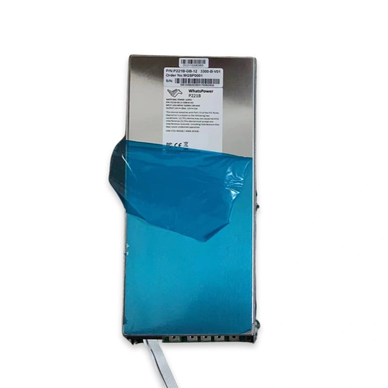
- Same PSU family — the BP-H-3640 PSU covers KS3, KS3L, KS3M, and the higher KS5L; the C19 power cord is shared across all four models
- Same chassis — the KS5M / KS5L / KS3M / KS3L miner case is a common form factor
The differentiator across KS3 models is the chip count per hashboard, which scales with the total miner hashrate. The KS3 (highest count) carries the most P2SG48 chips per board, the KS3M sits in the middle, and the KS3L carries the fewest. The diagnostic methodology and component inventory are identical across the three.
Note: The KS5L and KS5M use a different ASIC chip generation (1004LV100) and are not cross-compatible at the chip level with the KS3 family. The PSU, control board, fan, and chassis are shared, but the hashboard ASIC stock is separate. See our KS5L repair guide for the KS5-family components.
KS3L Hashboard Architecture at a Glance
The KS3L hashboard carries 56 P2SG48 ASIC chips arranged in 28 voltage domains × 4 chips per domain (versus the KS3 which carries 112 chips on the same 28-domain architecture — KS3L = half the chip count, half the hashrate). The whole KS3L miner consists of 3 hashboards (168 chips total) + 1 control board + BP-H-3640 PSU (or AP276 variant) + 4 cooling fans.
- 28 voltage domains × 4 ASIC chips per domain = 56 chips per board, 168 chips per whole miner
- P2SG48 ASIC chip operating voltage: approximately 0.4V during single-board testing (chip domain voltage)
- Boost circuit at chip position U15 (MP1517DR): converts the 15.5V PSU input to 17V on the KS3L (note: KS3 uses 12V→15.5V at U15; KS3L specifically uses 15.5V→17V because its PSU rail is already elevated). The U15 boost feeds the top 5 voltage domains (28, 27, 26, 25, 24) through their LDOs.
- Secondary boost stage (B628 / HX3608 / LN3608): supplementary step-up regulator that brings the auxiliary rail to 26V on KS3L (vs 22V on KS3) — measured at test point TP873.
- Lower domains (1-23) powering: the 2.2V input feeds the per-domain LDOs that output 1.8V.
- 0.8V rail: derived from the local 1.8V via the SGM2036-ADJ LDO.
- Per-chip voltage groups: each P2SG48 ASIC chip has three voltage references — domain voltage (~0.4V), VDDPST / VDDPLL1V8 (1.8V via MP2019 or SGM2036), and VDD0P8 / VDDPLL0V8 (0.8V via SGM2036).
- Signal routing: TX enters at IO pin 7 (3.3V), passes through level converter U8, then forward from chip 01 to chip 56 (1.8V operating). RX flows in reverse from chip 56 back to chip 01 through level converter U7. RSTN enters at IO pin 3, passes through level converter U6, then forward through the chain.
- Crystal oscillator: a 25 MHz T250 crystal is shared between every two chip levels (0.9V normal at the oscillator output).
- First-power-on ICs: when only the control board is powered, only U2, U3, U4, U5, U18, and U15 on the hashboard are powered. The current draw at this stage is ~0.08-0.1A.
KS3L power consumption variants by PSU + version combination
| Model | Firmware Version | PSU Model | Voltage | Power Consumption |
|---|---|---|---|---|
| KS3L | sy0811_ks3L_miner / sy0808_v2_ks3L_miner | BP-H-3640 | 14V | 2700W |
| KS3L | sy0811_ks3L_miner | AP276 | 13.5V | 2550W |
| KS3L | sy0808_v2_ks3L_miner | AP276 | 13V | 2410W |
| KS3 (reference) | All versions | — | 12V | 3200W |
The KS3L runs at ~5 TH/s nameplate hashrate (reaches stable hashrate 10-15 minutes after startup). The KS3 runs at ~8 TH/s. Operators should verify the firmware version (sy0811 vs sy0808_v2) and PSU model match to ensure expected power consumption.
The chip pin voltage measurements must be referenced to the "ground" of the current chip's voltage domain, not to the digital GND (0V), because the KS3 series uses voltage-division power delivery — measuring 1.8V against digital GND will read incorrectly because the current chip's "ground" is itself elevated above 0V by the cumulative domain voltage drop.
Most Common KS3L Hashboard Failure Modes
- 0 ASIC chips detected on the test fixture — walk the power chain: 12V/14V PSU output → MOS chip turn-on (T871 enable test point) → boost circuit output at TP872 = 17V (KS3L) and TP873 = 26V (KS3L) → per-domain LDO outputs (1.8V then 0.8V) → ASIC chip signal voltages. Reference values for KS3 are TP872 = 15.5V and TP873 = 22V — KS3L runs at higher boost voltages because its PSU input rail is already elevated to 14V.
- Specific chip count detected (chain stops at a specific position) — the chain is healthy up to that count and fails at the boundary chip. Use the DIR voltage method to identify the failed chip — measure DIR voltage at the next chip pin and read either 1.8V (PS0 pull-up suspect) or 0V (SP1 pull-down suspect); both should read 1.8V maximum at healthy chips.
- Hashboard not detected at all — usually a corrupted EEPROM or a failed clock from the T250 gold crystal oscillator. The T250 is shared across KS3M / KS3L / KS5L per the LYS product URL.
- High or low temperature fault reported by the miner — failed TMP75 temperature sensor producing implausible readings. Check the sensor IC and the 3.3V supply.
- Boost stage failure / 0 chips with bad rail voltage at TP872 — failed MP1517DR boost converter at U15 drops the elevated rail. Verify Vin / Vout / Ven / Vfb on the MP1517DR (Ven = 0V and Vfb = 0.6V are normal).
- Secondary boost stage failure — failed B628 (HX3608 / LN3608) power booster chip drops the auxiliary boost rail. The B628 is a step-up regulator IC paired with a dedicated inductor for KS3L auxiliary rail generation.
- Single-domain dropout — failed LDO (SGM2036-ADJ (SQ7JK) for 0.8V or MP2019 (SOP-8) for 1.8V) takes its local domain offline. Check the 1.8V and 0.8V at each chip pin against the current-domain ground reference.
- Signal-path level translation failure — failed SN74AUP1T34DCKR (U2E) on the TX / RX / RSTN level conversion path causes a block of downstream chips to drop offline simultaneously. Powering on the board in the wrong sequence (signal cable before positive rail) is the most common cause of U2-U18 destruction.
- Power-input protection failure — failed LMBR140T1G (S7) Schottky produces a short or open that disrupts the input rail.
- Current sense / shunt anomaly — degraded 1002 SMD resistor or 270R 1206 resistor in the current-sense network produces incorrect readings that trip protection.
- Output filter cap degradation under load — degraded 330µF 35V SMD or 47µF 50V SMD capacitors no longer hold rail voltage during transient draw. Visual inspection for swollen tops or leakage is the first check.
Critical Components — Function & Failure Behaviour
P2SG48 ASIC Hash Engine (KS3 family chip)
The KS3L uses the P2SG48 2329 Iceriver proprietary ASIC chip — the same chip as KS3 and KS3M hashboards (chip-level cross-compatible for repair stock across all three models). Each P2SG48 chip operates at approximately 0.4V domain voltage during single-board testing. ESD damage during handling and sustained thermal stress from dried thermal compound are the most common failure causes. The P2SG48 chip is sourced by quote — contact LYS at contact@lys-sz.com for stock check.
Primary Boost Converter (MP1517DR at U15)
The MP1517DR QFN-16 adjustable positive switching regulator at position U15 converts the 12V input to the elevated rail (15.5V or 17V depending on the model) that supplies the top 5 voltage domains. A failed MP1517DR drops the upper-domain rail and presents as 0 chips detected. Verify Vin / Vout / Ven / Vfb at U15 — Ven = 0V and Vfb = 0.6V are normal operating values.
Secondary Boost Stage (B628 / HX3608 / LN3608)
The B628 power booster chip (HX3608 / LN3608) is a supplementary step-up regulator paired with a dedicated inductor for auxiliary rail generation on the KS3L hashboard. If the secondary boost output drops while the primary MP1517DR rail at TP872 reads correctly, the B628 is the likely failure point.
Voltage Regulators (LDOs)
The KS3L uses the SGM2036-ADJ (SQ7JK) for the 0.8V chip core rail (VDD0P8 / VDDPLL0V8) and the MP2019 (SOP-8) for the 1.8V rail (VDDPST / VDDPLL1V8). A failed LDO takes its local chip group offline — measure both rails at each chip pin against the current-domain ground reference (not against digital GND).
Level Translators (U6 / U7 / U8)
The SN74AUP1T34DCKR (U2E) level translators handle TX (at U8), RX (at U7), and RSTN (at U6) signal conversion between the 3.3V control side and the 1.8V chip-side logic. A failed translator typically causes a block of downstream chips to drop offline at once — a useful diagnostic signature when scanning with the test fixture. Powering on the board in the wrong sequence (signal cable before positive rail) is the most common cause of U2-U18 destruction.
Temperature Sensor (TMP75)
The TMP75 digital temperature sensor monitors hashboard temperature. A failed sensor produces missing or implausible readings — the miner protection logic then trips on the bad reading and shuts the board down even if the actual temperature is healthy.
Crystal Oscillator (T250 Gold)
The T250 Gold Crystal Oscillator provides the 25 MHz timing reference, shared between every two chip levels. Normal voltage at the oscillator output is approximately 0.9V. A failed oscillator prevents chain initialisation entirely. The T250 is cross-shared across KS3M / KS3L / KS5L per the LYS product URL.
Protection & Storage
The LMBR140T1G (S7) Schottky diode handles freewheeling and reverse-polarity protection on the power-input stage. The EEFGX0D471R 470µF polymer capacitor handles bulk decoupling on the power-delivery rail, and the 10µH (Inductor 100 silkscreen) SMD inductor handles boost-stage energy storage paired with the MP1517DR and B628 boost converters.
Passive Components
The 330µF 35V SMD and 47µF 50V SMD electrolytic capacitors handle bulk decoupling on the power-delivery stage. The 47µF 50V SMD URL is KS3L-explicit (the LYS product slug names KS3L directly alongside S19 / S21 / T21). The 1002 SMD resistor and 270R 1206 resistor serve as current-sense / shunt and bias-network elements.
Iceriver KS3L Hashboard Repair Components List
The table below lists every component LYS Shenzhen stocks for KS3L hashboard repair. Each entry links directly to the corresponding part page — contact us at contact@lys-sz.com for the P2SG48 ASIC chip (sourced by quote), the 1002 SMD resistor, or for bulk farm-scale orders.
| Part Number | Component Type | Typical Position / Role |
|---|---|---|
| P2SG48 2329 ASIC Chip | Iceriver ASIC hash engine | KS3 family chip (cross-compatible KS3 / KS3L / KS3M) — contact us for stock check. KS3L-specific stencil: KS3M / KS3L tin tool |
| SN74AUP1T34DCKR U2E | Voltage level translator | U6 / U7 / U8 — TX / RX / RSTN signal conversion (3.3V ↔ 1.8V) |
| TMP75 | Temperature sensor | Digital hashboard temperature monitoring |
| T250 Crystal Oscillator (Gold) | Crystal oscillator | 25 MHz timing reference (shared between chip pairs) — cross-KS3M/KS3L/KS5L |
| SGM2036-ADJ (SQ7JK) | LDO regulator | 0.8V chip core rail (VDD0P8 / VDDPLL0V8) |
| MP1517DR | Boost converter IC | U15 — 12V → 15.5V/17V boost feeding top 5 domains |
| Inductor 100 (10µH) | SMD power inductor | Boost-stage energy storage paired with MP1517DR + B628 |
| MP2019 (SOP-8) | LDO regulator | 1.8V rail (VDDPST / VDDPLL1V8) |
| LMBR140T1G (S7) | Schottky diode | Power-input freewheeling and reverse-polarity protection |
| 1002 SMD Resistor | Resistor | Current-sense / shunt — contact us for stock check |
| 270R SMD 1206 Resistor | Resistor | Bias-network element — contact us for stock check |
| 47µF 50V SMD | Electrolytic capacitor | Local rail decoupling — KS3L-explicit listing on Shopify |
| 330µF 35V SMD | Electrolytic capacitor | Bulk filtering on power stage |
| B628 (HX3608 / LN3608) | Power booster chip | Secondary step-up regulator for auxiliary rail generation |
| EEFGX0D471R 470µF | Polymer capacitor | Bulk decoupling on power-delivery rail |
Required Repair Tools & Consumables
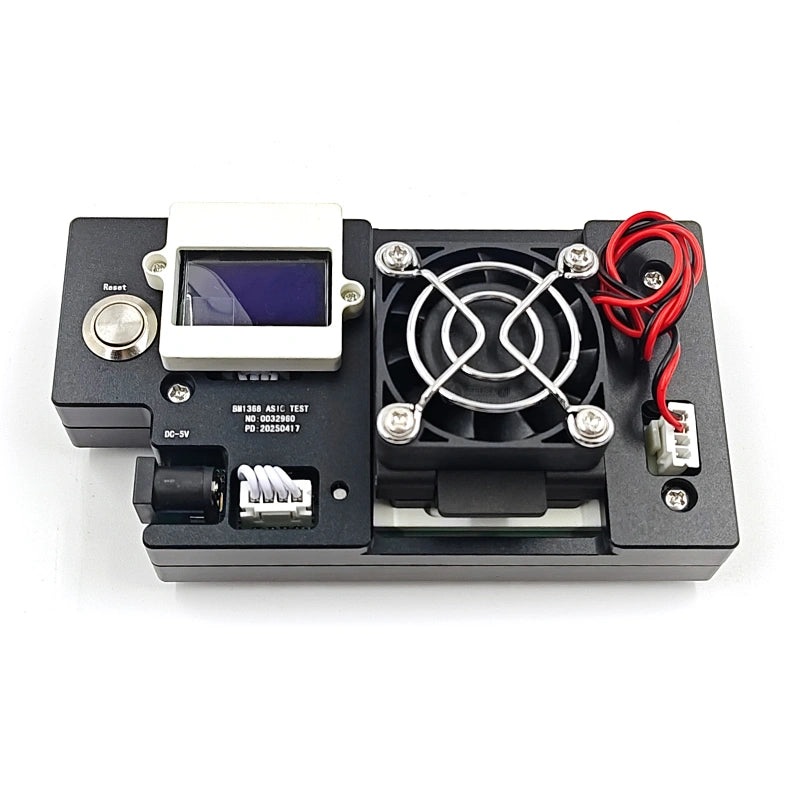
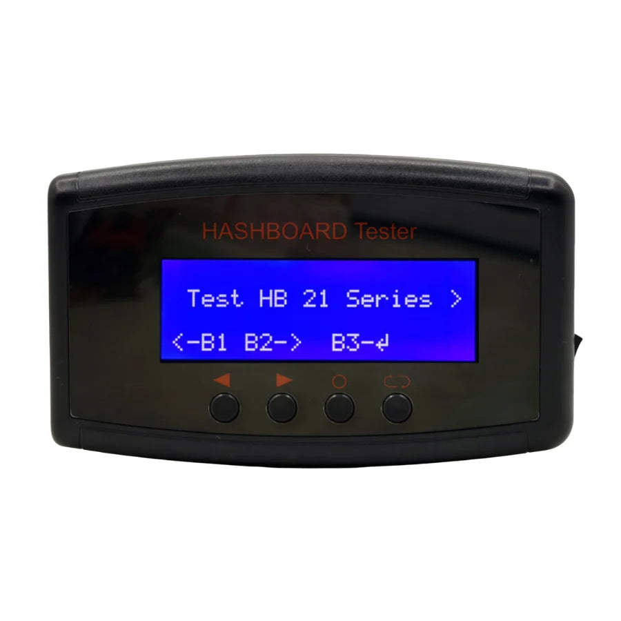
- Iceriver KS-series test fixture — the dedicated KS-series hashboard test fixture is required for chip-level fault isolation on the KS3L (the same fixture family covers KS3 / KS3L / KS3M).
- Iceriver KS3M / KS3L tin tool (P2SG48 stencil) — dedicated reballing stencil for the KS3-family chip footprint, KS3L-explicit URL.
- Iceriver 4-pin fan simulator — allows the miner control board to start without physical fans during bench testing.
- Regulated bench PSU: 12V fixed voltage, current limit at 2A for KS3L-class boards. Bench power-up current at first power = ~0.1A (control board only), rises to ~0.9A on enable, then to ~1.8A during full chain test.
- Constant-temperature soldering iron at 350-400°C for SMT work.
- Hot-air rework station rated 350-400°C for chip removal.
- Solder paste M705 grade, no-clean flux, board washing fluid with anhydrous alcohol.
- Multimeter (Fluke 15B+ recommended), tweezers, electric screwdriver, short-circuit probe wire.
- High-temperature adhesive tape — protect electrolytic capacitors and LEDs during nearby rework.
- Thermal compound rated 5W/mK or higher for heatsink interface.
- Quick-drying three-proof paint for both sides of the LDO chips after repair.
- Common spare 0402 resistors (0R, 10K) and 0402 capacitors (1µF), plus 0603 resistors (33R) and 0603 capacitors (1µF / 22µF).
KS3L Diagnostic Workflow
Pre-power inspection
- Visual: check PCB for deformation, scorching, displaced or missing components, solder bridges around the boost stages.
- Resistance: measure 12V input to GND for short. Measure 1.8V and 0.8V rails to their domain ground for shorts.
- Connector: check the IO ribbon connector for damaged or bent pins.
Power-up sequence (mandatory — wrong order destroys U2-U18 level translators)
- Connect negative copper rail first.
- Connect positive copper rail second.
- Connect signal cable last.
- Apply 12V from bench PSU at 2A current limit.
- For shutdown: reverse order — signal cable off first, then positive, then negative.
Power-rail verification
- Step 1 — 12V input check. Verify bench PSU output reaches the hashboard 12V input terminal.
- Step 2 — MOS enable check at T871. Verify MOS chip turn-on enable voltage at T871 test point.
- Step 3 — Primary boost at TP872. Measure 15.5V at TP872 (MP1517DR output). If missing, check Vin / Vout / Ven / Vfb at the MP1517DR.
- Step 4 — Secondary boost. Measure 22V at TP873. If missing, check the B628 power booster chip and its associated inductor.
- Step 5 — Per-domain LDO outputs. Verify 1.8V (MP2019) and 0.8V (SGM2036-ADJ) at each chip pin against the current-domain ground reference, not against digital GND.
- Step 6 — Crystal oscillator. Verify ~0.9V at the T250 output for each chip pair.
- Step 7 — Signal-path level conversion. Verify 1.8V at TX / RX / RSTN paths through U6 / U7 / U8 after level conversion from 3.3V input.
Chip-level dichotomy localisation
When the test fixture reports a specific chip count (chain stops at chip N), the bad chip is at position N+1. Use the DIR voltage diagnostic method to confirm: measure DIR voltage at the suspect chip pin while the single-board test program is running. Result is either 1.8V or 0V.
- If DIR = 1.8V: use a short-circuit wire to pull up the PS0 pin of the ASIC chip. Important: pull-up voltage can only be 1.8V — higher voltage will damage the chip.
- If DIR = 0V: use a short-circuit wire to pull up the SP1 pin of the ASIC chip. Same 1.8V pull-up rule.
- Observe single-board test program results. If the count advances by 1, the previous chip was the boundary. If still garbled, move one chip level higher and repeat the DIR test + PS0/SP1 pull-up until you find the bad chip.
DIR voltage resistance table (chip-pin reference values)
Use a multimeter in resistance mode to check chip-pin resistance values relative to the current voltage domain — both DIR=1.8V and DIR=0V scenarios have distinct expected values per pin pair:
| Test point pair | DIR = 1.8V (expected resistance) | DIR = 0V (expected resistance) |
|---|---|---|
| NK1-NK1 | ~2 kΩ | ~13 MΩ |
| SP1-SP1 | ~7-12 MΩ | ~7-12 MΩ |
| RT1-RT1 | ~12 kΩ (chips 1-4: ~0.4 MΩ) | ~15 MΩ |
| TR1-TR1 | ~15 MΩ (chips 1-4: ~40 MΩ) | ~12 kΩ |
| PS1-PS1 | ~7-12 MΩ | ~7-12 MΩ |
| KN1-KN1 | ~13 MΩ | ~2 kΩ |
If measured resistance deviates significantly from the expected value, the chip in question (or its immediate surrounding circuit) has failed.
For chip replacement, use the KS3M / KS3L tin tool (P2SG48 stencil) to pre-tin the chip pads with M705 paste. Protect nearby electrolytic capacitors and LEDs with high-temperature adhesive tape during rework. After chip replacement, apply fresh thermal compound (5W/mK minimum) to the heatsink interface before reassembling.
Control board test points
If the whole machine cannot start or login to the web backend, check the control board:
- TP3 = 1.0V; TP4 = 1.8V; TP5 = 1.5V; TP6 = 3.3V — all four must read within spec.
- Blue LEDs at positions D1 + D6 should both be on. If only D6 is on and current is ~0.08-0.1A, the system has not started — check SOC, DDR, FLASH.
- R22 resistor voltage: ~0.69V both sides = FLASH and SOC are normal (likely DDR fault if system still won't boot). ~1.5V both sides = FLASH program corrupted or FLASH damaged. Higher than this current indicates a short-circuited component in the circuit.
Post-Repair Validation
- Reinstall hashboard into KS3L chassis (verify connector orientation).
- Apply 12V from bench PSU with 2A current limit OR install into the BP-H-3640 PSU + chassis assembly.
- Connect to control board via signal cable (signal cable LAST per power-on sequence).
- Apply power and monitor current draw: ~0.1A at first power (control board only) → ~0.9A on enable → ~1.8A during full chain test.
- Run full chain test via the Iceriver test fixture. All P2SG48 chips must report green.
- Run a 2-hour soak test at full hashrate before clearing the hashboard for customer return.
When Chip-Level Repair Makes More Sense Than Replacement
New KS3L hashboard stock is increasingly constrained — Iceriver's volume production for the KS3 generation has tapered, and the secondary market is mostly other operators' failed boards. For KAS / Kaspa fleet operators running KS3-family miners, component-level repair is the realistic path. A small inventory of the P2SG48 ASIC chip, the MP1517DR + B628 boost converters, the SGM2036-ADJ + MP2019 LDOs, the SN74AUP1T34 level translators, the TMP75 temperature sensor, the T250 crystal oscillator, the LMBR140T1G Schottky, and the 47µF / 330µF SMD capacitors covers the majority of bench-repair scenarios on KS3L boards.
Several KS3L components are shared across other miners — MP1517DR with the Antminer S17 / T17 / S19 / T19, MP2019 with the S17 / T17 / S19, SN74AUP1T34 with the L7 + S19, TMP75 with the Antminer hashboard family. A repair bench already stocking parts for the Antminer Bitmain line can extend coverage to the KS3 family with relatively few additions.
FAQ — Iceriver KS3L Hashboard Repair
What ASIC chip does the KS3L use?
The KS3L uses the P2SG48 2329 Iceriver proprietary ASIC chip — the same chip platform as the KS3 and KS3M (cross-compatible across all three KS3-family models). Each chip operates at approximately 0.4V domain voltage. P2SG48 chips are stocked by quote at LYS Shenzhen.
What is the difference between KS3L, KS3M, and KS3?
All three models use the same P2SG48 ASIC chip, the same 28-voltage-domain hashboard topology, the same BP-H-3640 PSU, the same control board, the same cooling fan, and the same chassis. The differentiator is chip count per hashboard, which scales with total miner hashrate: KS3 (highest) → KS3M (mid) → KS3L (entry-tier, lowest). The repair methodology and component inventory are identical across the three.
Is the KS3L chip cross-compatible with the KS5L?
No. The KS3 family (KS3 / KS3L / KS3M) uses the P2SG48 ASIC chip. The KS5 family (KS5L / KS5M) uses the 1004LV100 ASIC chip — a different generation. The PSU, control board, fan, and chassis are shared, but the hashboard ASIC stock is separate. Plan inventory accordingly when running mixed KS3 + KS5 fleets.
What is the correct power-on sequence for KS3L hashboard repair?
Negative copper rail first → positive copper rail second → signal cable last. Power-off is the reverse: signal cable first → positive copper → negative copper. Wrong order destroys U6 / U7 / U8 (SN74AUP1T34DCKR level translators), which is the most common bench-error cause of KS3L hashboard failure after repair.
How do I localise a bad chip on the KS3L hashboard?
When the test fixture reports a specific chip count, the bad chip is at position N+1. Use the DIR voltage diagnostic method: measure DIR voltage at the suspect chip pin. If DIR = 1.8V → PS0 pull-up suspect. If DIR = 0V → SP1 pull-down suspect. Both should read 1.8V maximum at healthy chips.
Why does the KS3L use two boost converters (MP1517DR + B628)?
The MP1517DR primary boost converter at U15 converts 12V → 15.5V/17V to feed the top 5 voltage domains via their LDOs (test point TP872). The B628 (HX3608 / LN3608) secondary boost chip generates an auxiliary rail (typically 22V at TP873) for additional power-delivery requirements specific to the KS3L hashboard topology.
Why must I reference voltage measurements to the current chip's domain ground?
The KS3 family uses voltage-division power delivery — each chip's "ground" is itself elevated above digital 0V by the cumulative domain voltage drop from chip 1 to the current chip. Measuring 1.8V VDDPLL or 0.8V VDD0P8 against digital GND (0V) will read incorrectly. Always reference the measurement against the current chip's local ground pin to get an accurate reading.
Is the KS3L still profitable to repair in 2026?
Yes — KAS / Kaspa mining economics remain positive in low-power-cost regions, and the KS3L's lower power draw makes it well-suited to entry-tier fleet operators. With most KS3L units now 2-3 years into service, component-level repair on the existing fleet is the realistic path. Contact LYS Shenzhen at contact@lys-sz.com for parts pricing and bulk supply.
Sourcing KS3L Hashboard Repair Parts
LYS Shenzhen stocks every component listed above for the Iceriver KS3L hashboard, including the P2SG48 ASIC chip (sourced by quote due to demand variability) and the matching KS3M / KS3L tin tool stencil. For the broader Iceriver KS lineup (KS3, KS3M, KS5L, KS5M), or for KS3L complete-miner sourcing, contact our team at contact@lys-sz.com — we operate an on-demand sourcing channel for repair components across the full Iceriver KAS-mining miner range.
Worldwide shipping from our Shenzhen warehouse via DHL, FedEx, UPS, and sea freight. DDP shipping available for US and EU customers; case-by-case for other lanes — request a quote with your shipping country for confirmation.