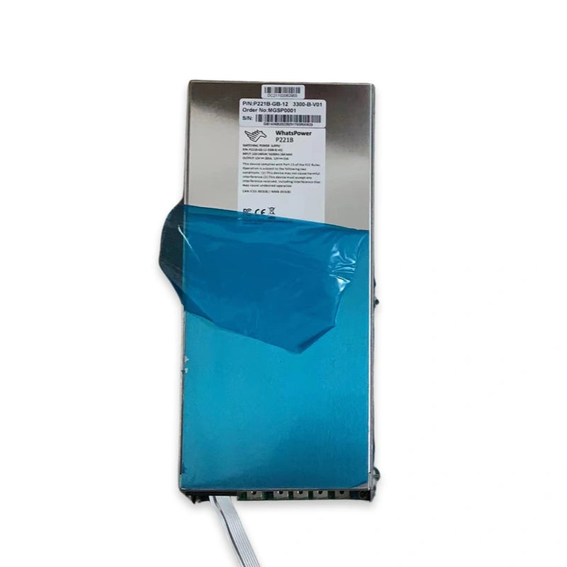
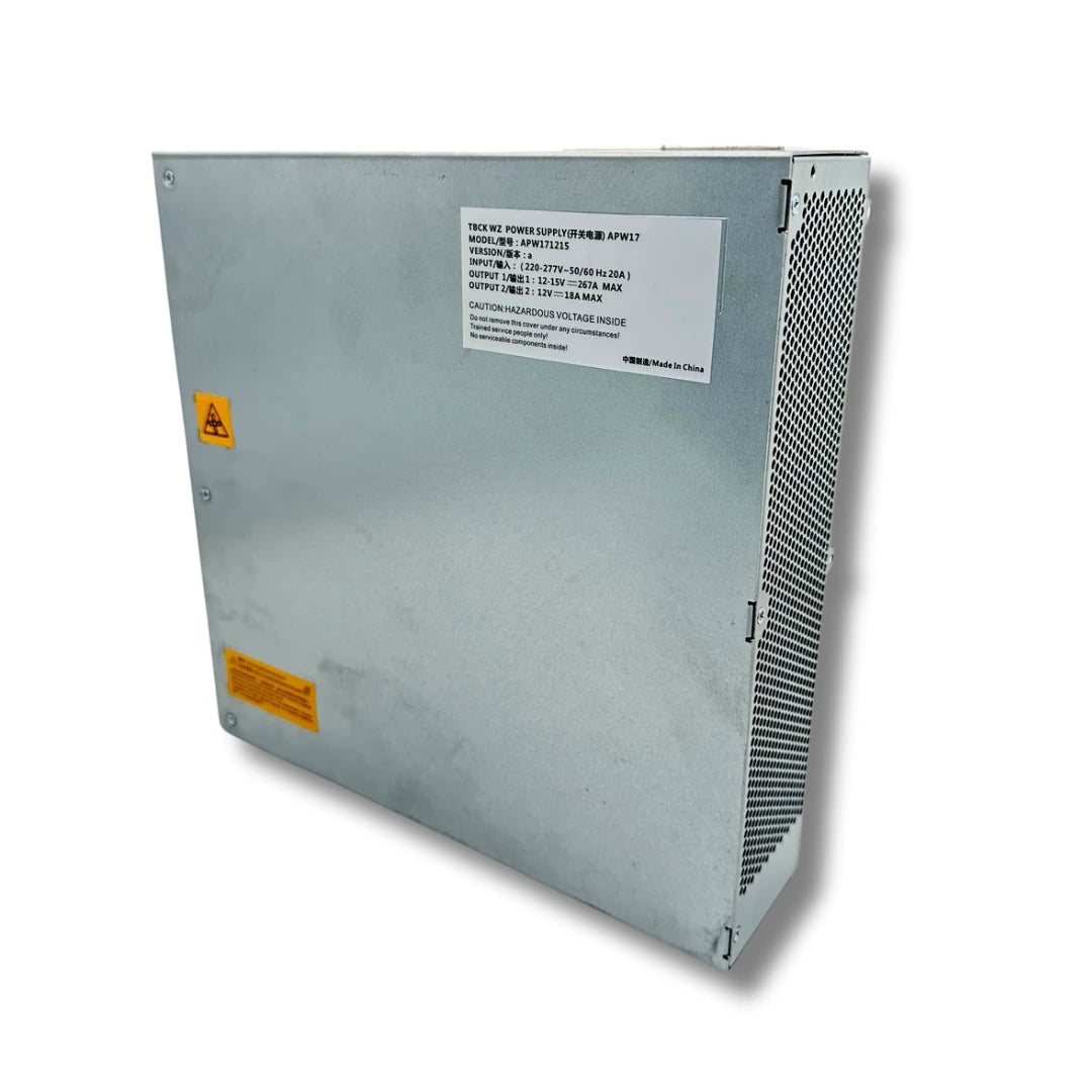
Bitmain APW7 Power Supply Unit Repair Guide & Components List (2026 Update)
The Bitmain APW7 — formally the APW7-12-1800 series — is the legacy single-output PSU that powered the Antminer S9 and L3 generations. Built around a PFC + LLC half-bridge topology with the ICE2QR4765 quasi-resonant controller and the FAN7688SJX secondary-side synchronous rectification controller, the APW7 ships a single 12V rail at 1800W from a universal 200-264V AC input. Many APW7 units are still running across older S9 / L3 fleets in low-cost-power environments. This guide covers the 18 most vulnerable components, the Bitmain-documented diagnostic workflow, and the full repair playbook with direct sourcing links — completing the Bitmain APW PSU family coverage alongside our APW8 (S15/T15), APW9 / APW9+ (S17), and APW12 (S19) repair guides.
Why APW7 PSU Repair Matters in 2026
The APW7 powered the largest single fleet of Antminers ever shipped — the S9 series — across years of production. Many S9 units remain in operation today in markets with very low electricity costs, where the modest hashrate is still profitable. Replacement APW7 units have been out of Bitmain volume production for years; component-level repair is the only realistic path to keep these PSUs alive. Most APW7 failures trace back to aged primary MOSFETs, a degraded bulk capacitor, or the well-documented R33 voltage-detection-startup resistor failure — all replaceable parts with available repair stock.
Compatible Antminer Models
The APW7 series powered the following Antminer models:
- S9 family: S9 (~14 TH/s), S9i, S9j, S9k, S9 SE, S9-Hydro variants — the most widely deployed Bitmain miner in history
- L3 family: L3+, L3++ — early-generation Scrypt miners for Litecoin / Dogecoin
- Other legacy Antminer: select S7, T9, T9+ and similar S9-era miners that used a 12V single rail PSU
The APW7 ships a single 12V DC output at 1800W via 10 PCIE 6-pin connectors on a 380mm output cable. This single-rail architecture distinguishes it from the later APW8 / APW9 / APW9+ / APW12 family, which all carry a variable main rail plus a separate 12V auxiliary. The APW7 is not directly interchangeable with newer PSU generations — the output topology, the connector format (10× PCIE vs M6 copper-bar), and the voltage range are all PSU-generation-specific.
The APW3++ predecessor is deprecated and not in active production for repair stock. For the newer S15-class PSU, see our APW8 PSU repair guide.
APW7 PSU Architecture at a Glance
The APW7 is a PFC-fronted LLC half-bridge switching supply with secondary-side synchronous rectification. Bitmain's documented architecture is: AC input 200-264V → EMI filter → rectifier bridge → PFC stage → VBUS large capacitor → LLC main switch (half-bridge) → main transformer → secondary synchronous rectification → 12V DC output. A separate auxiliary supply (T1 transformer) provides VCC for the primary and secondary control ICs plus fan power.
Specifications (APW7-12-1800)
- AC input: 200-264V universal, single-phase, C14 connector (requires C13 AC cable)
- DC output: 12V single rail at 1800W (full power on 200-240V input). Derated to ~1000W on 110V input.
- Output current: rated 150A continuous, OCP trips at 160-200A
- Power factor: >0.99 at full load
- Maximum conversion efficiency: 95% (excluding output cable loss)
- Output ripple: <1%
- Output cable: 10× PCIE 6-pin connectors, 380mm length (yellow 1/2/3 positive, black 4/5/6 negative)
- Protection: under-voltage, short-circuit, overload, over-temperature, with automatic recovery after fault removal
- Operating temperature: full-load operation up to 60°C ambient
Component-level architecture
- Input stage: F1 fuse, U2 rectifier bridge (GBJ2506 25A / 600V), NTC 10D-15 inrush thermistor, varistor on the AC line, and an inrush relay that bypasses the NTC once the bulk cap is charged.
- PFC stage: Q4 (also referenced as Q1) PFC switch MOS with D5 / D6 / D7 PFC diodes. The PFC large capacitor (positions C16 / C17) holds the bus voltage at 375-385V DC during normal operation.
- Auxiliary 12V supply: U5 drive switch integrated chip (pins 3 and 4 must not be shorted), T1 auxiliary transformer, Q5 main switch MOS, D6 / D7 / D8 / D9 / D11 rectifiers, R37 / R38 sense resistors. The auxiliary winding outputs VCC 12V1 to the primary-side control IC and a separate 12V2 to the fan / secondary-side control IC. Voltage feedback is sampled and regulated via an opto-isolated loop.
- LLC main switching: Q6, Q14, Q15, Q16 form the primary half-bridge. Built around TK39N50W5 (K39N60W series, 600V N-channel), IPA60R060P7 (high-voltage N-channel), and OSG65R099HZ (high-voltage N-channel).
- Quasi-resonant control: ICE2QR4765 quasi-resonant offline PWM controller (650V) drives the primary stage. Same controller is shared with the APW3 and APW12 lines.
- PWM main drive: U10 is the PWM main control driver IC — pin 15 must read 12V VCC and pin 1 must read 5V reference for the IC to operate. Additional PWM drive ICs at U11 and U12.
- Gate driver: IX4424NTR / IX4424N dual low-side MOSFET driver (8-pin SOIC) — shared with APW8 and APW9. FAN3224T dual 4A high-speed low-side gate driver completes the gate-drive chain.
- Drive isolation transformer: T4 isolates the PWM drive signal between primary and secondary sides.
- Secondary-side controller: FAN7688SJX secondary-side synchronous rectifier controller (16-SOP) drives the output sync MOSFETs.
- Synchronous rectification (output): Q17, Q18, Q19, Q20 output sync MOSFETs. Built around 5C404N (NVMFS5C404N, 40V / 378A N-channel) and TPHR8504PL (40V N-channel, shared APW7/8/9/12).
- Output rectifier: SCS210AM 650V / 10A SiC diode on the secondary path.
- Bulk capacitance: 450V 470µF (30×45mm, 1850mA, 2000h @ 105°C) primary DC bus; 1000µF 16V output filter capacitors.
- Voltage reference / feedback: ZTL431BFTA adjustable shunt voltage reference (2.5V / 100mA, SOT-23-3) sets the output regulation point.
- Sampling / feedback amplifier: LM358 dual general-purpose op-amp (8-SOIC) on the sampling and feedback paths.
- Small-signal support: DSS5540X (-13) PNP BJT (40V / 4A, SOT-89) and MMBT3904 (1AM) NPN transistor handle protection-circuit support.
Most Common APW7 PSU Failure Modes
- No DC output, fan spinning, AC LED green — first check the PCIE 6-pin output connectors and the harness for damaged terminals or oxidised ring lugs. A loose ring lug on a PCIE connector presents identically to a dead PSU on the load side.
- PSU dead after AC input, fan does not start — check the F1 fuse first. A blown fuse usually points to a downstream short on the primary switching stage (TK39N50W5 / IPA60R060P7 / OSG65R099HZ MOSFETs at the Q6 / Q14 / Q15 / Q16 positions).
- Hard short on primary switching — typically a failed TK39N50W5, IPA60R060P7, or OSG65R099HZ MOSFET. Test in diode mode before powering up — a healthy MOSFET shows 0.3-0.6V drop between drain and source.
- Quasi-resonant controller fault — failed ICE2QR4765 prevents the primary stage from oscillating; no switching means no transformer output.
- Auxiliary 12V dead — fan not rotating — focus on U5 drive switch IC (check pins 3 and 4 for short), R37 / R38 (drift or open), T1 transformer (check primary and secondary windings for open), and Q5 / D6 / D7 / D8 / D9 for damage.
- Output voltage out of spec — degraded ZTL431BFTA voltage reference drifts the regulation point. Inspect the LM358 sampling op-amp if reference is healthy but output still drifts.
- Secondary sync rectification failure — failed 5C404N (NVMFS5C404N) or TPHR8504PL sync MOSFET produces low / unstable output voltage. Verify the FAN7688SJX secondary-side controller has correct VCC if multiple sync MOSFETs appear healthy.
- Output voltage drops under load — degraded 1000µF 16V output capacitors no longer hold rail voltage during transient draw. Visual inspection for swollen tops or leaked electrolyte is the first check.
- Bulk capacitor failure / primary instability — degraded 450V 470µF bulk capacitor produces ripple on the primary DC rail. Bitmain spec is 1850mA ripple / 2000h @ 105°C — replacement caps must meet or exceed this spec.
- PWM main drive fault — measure U10 pin 15 = 12V VCC and pin 1 = 5V reference. Either rail missing indicates the auxiliary supply chain or U10 itself has failed.
Bitmain APW7 PSU Repair Components List
The table below lists every component LYS Shenzhen stocks for APW7 PSU repair. Each entry links directly to the corresponding part page — contact us at contact@lys-sz.com for bulk pricing or for complete APW7 PSU replacement units.
| Part Number | Component Type | Typical Position / Role |
|---|---|---|
| ICE2QR4765 | AC/DC quasi-resonant PWM controller | 650V offline primary stage controller |
| ZTL431BFTA | Voltage reference | Adjustable shunt 2.5V / 100mA, SOT-23-3 — output regulation |
| IX4424NTR / IX4424N | Gate driver | Dual low-side MOSFET driver, 8-SOIC (shared APW7/8/9) |
| DSS5540X (-13) | PNP BJT transistor | 40V / 4A, SOT-89 — gate-drive / protection support |
| TK39N50W5 | N-channel MOSFET | TO-247, 600V / 38.8A primary switching (Q6/Q14/Q15/Q16) |
| 1000µF 16V | Electrolytic capacitor | Output bulk filtering |
| 5C404N (NVMFS5C404N) | N-channel MOSFET | 40V / 378A output synchronous rectification (Q17-Q20) |
| SCS210AM | SiC Schottky diode | 650V / 10A TO-220FM secondary rectification |
| TPHR8504PL | N-channel MOSFET | 40V synchronous rectification (shared APW7/8/9/12) |
| MMBT3904 (1AM) | NPN transistor | Small-signal switching on protection stage (shared APW3/APW7) |
| GBJ2506 | Bridge rectifier | 25A / 600V single-phase input (U2) |
| 60R060P7 (IPA60R060P7) | N-channel MOSFET | High-voltage primary switching |
| NTC 10D-15 | Thermistor | 10Ω / 15mm inrush current limiter (shared APW3/APW7) |
| 450V 470µF | Electrolytic capacitor | Primary DC bus bulk (30×45mm, 1850mA, 2000h @ 105°C) |
| FAN7688SJX | Secondary-side controller | 16-SOP synchronous rectifier controller (output stage) |
| LM358 | Operational amplifier | Dual general-purpose, 8-SOIC — sampling / feedback |
| OSG65R099HZ | N-channel MOSFET | High-voltage primary switching |
| FAN3224T | Gate driver | Dual 4A high-speed low-side, gate-drive chain |
Diagnostic and Repair Workflow — 6-Step Bitmain-Documented Procedure
Bench setup requirements
- AC controllable power supply / voltage regulator: output 200-250V, current limit 0-20A. If unavailable, a 100W ordinary light bulb in series with the AC line bus can serve as a current-limiter (with caution).
- Electronic load: 2KW capable, 0-50V. If unavailable, a resistive load matched to the APW7 spec can substitute.
- Power analyzer: for power factor and power measurement after repair.
- Multimeter: Fluke 15B+ recommended.
- Soldering equipment: 80W+ constant-temperature soldering iron with tip head (300-350°C for chip resistors / capacitors) and blade head (380-420°C for plug-in components). Thermal chimney / hot-air station at 260°C ±2°C for chip removal.
- Auxiliary materials: thermal silicone grease 2500 for MOSFET-to-heatsink interface, 704 silica gel for protective glue replacement, lead-free solder wire, flux, anhydrous alcohol for board cleaning.
Safety — mandatory before opening the case
The bulk capacitor must be discharged before any soldering operation. Verify the residual voltage with a multimeter — the cap must measure below 5V before you touch the board. After AC disconnect, wait for the fan to stop completely before touching the board (this confirms the bulk cap has discharged through the bleeder). Wear an anti-static wrist strap, work on a grounded anti-static workbench.
6-step diagnostic procedure
- Step 1 — External visual inspection. Check the appearance is not seriously damaged or deformed, and the DC fan and AC socket are not damaged. Fix obvious external issues first.
- Step 2 — Apply AC 220V and check basic operation. Verify the fan rotates normally. Use a multimeter to check the J6 output terminal voltage = 12V (range 12.1-12.5V acceptable for measurement tolerance). This confirms the 12V output and the auxiliary supply chain are functional.
- Step 3 — Open the enclosure and inspect for sparking. After discharging the bulk capacitor below 5V, open the case. Look for sparking marks on components or solder surface. Pay particular attention to R33 — this is a known failure point. Use the multimeter to check: F1 fuse for open circuit; U2 rectifier bridge integrity; PFC MOS at Q4 (Q1) and PFC diodes D5 / D6 / D7 for shorts; main switch MOSFETs Q6 / Q14 / Q15 / Q16 for shorts; output sync MOSFETs Q17 / Q18 / Q19 / Q20 for shorts. Any short = check and replace, inspecting surrounding small-signal transistors that may be damaged alongside.
- Step 4 — Verify the auxiliary 12V circuit. Test U5 drive switch IC (pins 3 and 4 must not be shorted), T1 12V transformer (check windings for open), Q5 main switch MOS, D11 rectifier diode, and surrounding components for damage. If the fan doesn't rotate but the rest of the PSU appears healthy, focus on this stage first — without the auxiliary 12V, neither the primary control IC nor the secondary control IC will operate.
- Step 5 — Verify PFC bus, main control, and PWM drive. If F1 fuse path is normal and AC powers up the fan and produces 12V at J6: measure the PFC large capacitor C16 / C17 — should read 370-380V DC across. If absent, check U1 pin 7 VCC = 12V (replace U1 if damaged). If U1 VCC is healthy but the PFC bus is missing, check the PWM circuit ICs U9, U10, U11 for correct 12V VCC supply, and specifically verify U10 pin 15 = 12V and pin 1 = 5V reference. Replace any failed PWM IC. Then check the T4 drive transformer for damage.
- Step 6 — Skill-based judgment. Other defects need further analysis based on maintenance personnel experience. For unclear faults, use an oscilloscope to inspect the LLC switching waveform on the primary side and the synchronous rectification waveform on the secondary side.
Key test point voltages (Bitmain reference)
- PFC large capacitor (C16 / C17): 370-380V DC under normal operation (some Bitmain references cite 375-385V — both ranges are acceptable bracketing the same target).
- J6 12V output: 12V (12.1-12.5V acceptable to absorb measurement tolerance).
- U1 pin 7 VCC: 12V (powers the primary-side main control IC).
- U10 pin 15: 12V VCC (PWM main control driver IC).
- U10 pin 1: 5V reference (PWM control reference voltage).
- U9 / U11 / U12 VCC: 12V (PWM circuit support).
Electrical Function Test (Post-Repair Validation)
Bitmain's documented function test runs at two AC input voltages to verify the universal-input design works within spec:
- Visual inspect the board: no pseudo soldering, continuous soldering, wrong-polarity electrolytic capacitor, missing plug-in components, displaced MOS insulating gaskets. Connect AC L/N input and DC output ± terminals.
- Turn on AC input. Set the electronic load to 1A and confirm the output voltage reads 12.10-12.50V = OK.
- At 220V AC input: set the electronic load to 150A. Record voltage, power, and power factor on the AC-side power meter. Qualified if PF >0.99, output voltage normal, power ≥1800W. Then increase the load 2A per step — the OCP should trigger between 160-200A. After OCP triggers, cycle AC and verify the PSU restarts normally.
- At 110V AC input: set the electronic load to 83.3A. Record voltage, power, and PF. Qualified if PF >0.99, output voltage normal, power ≥1000W (the APW7 derates on 110V input — full 1800W requires 220V).
- Turn off AC and load, remove AC input and DC output lines. Wait for the fan to stop completely before touching the board (bulk capacitor discharge confirmation).
If full power-meter / electronic-load setup is unavailable, the simplified test is: input AC 220V + output 12V plus 150A load (1800W). Operating normally under that load is considered qualified.
Mandatory post-repair soak test
After the function test confirms the PSU is healthy, run a minimum 2-hour soak test at 80% rated load (130A or more) before considering the unit cleared for customer use. This catches latent failures that survive the initial bench test but fail under sustained thermal stress.
When Chip-Level Repair Makes More Sense Than Replacement
New APW7 PSU stock is increasingly constrained — Bitmain stopped volume manufacturing this generation years ago. For S9 / L3 fleet operators, component-level repair is often the only realistic path. A small inventory of the primary MOSFETs (TK39N50W5, IPA60R060P7, OSG65R099HZ), the secondary MOSFETs (5C404N, TPHR8504PL), the ICE2QR4765 quasi-resonant controller, the FAN7688SJX secondary-side controller, the gate drivers (IX4424NTR, FAN3224T), the SCS210AM SiC diode, and the bulk capacitors covers the majority of bench-repair scenarios. Many components are shared with the APW8 PSU and the APW3 line — a single stock covers APW3 / APW7 / APW8 / APW9 / APW12 repair needs across the older Bitmain PSU range (see cross-platform component sharing matrix in the APW8 article).
FAQ — Bitmain APW7 PSU Repair
Which Antminer models use the APW7 PSU?
The APW7 is the PSU for the Antminer S9 family (S9, S9i, S9j, S9k, S9 SE, S9-Hydro variants) and the L3 family (L3+, L3++), plus select S7 / T9 / T9+ legacy units. It delivers a single 12V rail at 1800W from a universal 200-264V AC input. Newer S15 / T15 miners use the APW8 (16-20V); S17-class miners use the APW9 / APW9+ (14.5-21V); S19-class miners use the APW12 (12-15V).
What topology does the APW7 use?
The APW7 is a PFC-fronted LLC half-bridge switching supply with secondary-side synchronous rectification. The primary stage is driven by the ICE2QR4765 quasi-resonant offline PWM controller (same controller is shared with the APW3 and APW12). The secondary side uses the FAN7688SJX synchronous rectifier controller to drive the output sync MOSFETs. Output is a single 12V rail at 1800W via 10× PCIE 6-pin connectors.
What is the OCP (overcurrent protection) threshold on the APW7?
The APW7 rated output is 150A continuous; the OCP triggers between 160A and 200A depending on production variant. After OCP triggers, the PSU latches off until AC power is cycled — at which point it should restart normally.
Why does the APW7 deliver only 1000W on 110V input vs 1800W on 220V?
The APW7 ships with a universal 200-264V AC input but is derated on 110V mains. At 220V AC input, it delivers full 1800W rated power. At 110V AC input, the spec is approximately 83.3A at 12V (about 1000W). This derating is by design — the input current rating limits the power transfer at low input voltage.
How do I test the APW7 after repair?
The Bitmain function test runs at two AC voltages: 220V (full 1800W load = 150A, PF >0.99) and 110V (~1000W load = 83.3A). After the function test passes, run a 2-hour soak test at 80% rated load (130A or more) before considering the PSU cleared for customer use. Without an electronic load, a known-good S9 chassis can substitute as a fixed-load test.
Sourcing APW7 PSU Repair Parts
LYS Shenzhen stocks every component listed above for the Bitmain APW7 PSU. For complete APW7 PSU replacement units, for bulk farm-scale orders, or for the broader Antminer PSU lineup (APW8, APW9, APW9+, APW11, APW12, APW17), contact our team at contact@lys-sz.com — we operate an on-demand sourcing channel for repair components across the full Bitmain PSU generation range.
Worldwide shipping from our Shenzhen warehouse via DHL, FedEx, UPS, and sea freight. DDP shipping available for US and EU customers; case-by-case for other lanes — request a quote with your shipping country for confirmation.