Antminer D7 Hashboard Repair Guide & Components List (2026 Update)
The Bitmain Antminer D7 is the workhorse X11 ASIC miner for Dash mining, built around the BM1764 ASIC chip in a BXD34601 hashboard layout — 70 chips per board, 35 voltage domains, 3 boards per miner, ~1286 GH/s nameplate at ~3148W power draw. Released in 2021, the D7 fleet is now in its 5th year of service and component-level repair is the primary path to keep these miners producing. This guide covers the 26 most vulnerable D7 hashboard components, the Bitmain-documented 6-step diagnostic workflow including the dichotomy test method, signal-direction tracing (CLK/RST/RX/BO), the boost circuit + LDO chain, the PIC microcontroller programming procedure, and the full repair playbook with direct sourcing links — complementing our Antminer L7 (Scrypt) repair guide as the Bitmain X11 / Scrypt altcoin mining repair reference.
Why D7 Hashboard Repair Matters in 2026
The Antminer D7 powered most of the institutional Dash mining capacity through the X11 mining cycle. As of 2026, the Dash network economics have compressed — block reward and mining margin are tight, and the D7 sits in the "operate the existing fleet rather than buy new" zone for most operators. Replacement D7 hashboards are scarce on the secondary market and Bitmain stopped volume production years ago. The realistic path is component-level repair: a small inventory of the BM1764 ASIC chips, the boost circuit MOSFETs (TPHR9003NL, MDU3603), the LDO chain (SGM2036 family, MP2019GN), the level translators (74AUP1T34, NLSV1T34), the PIC supervision IC, and the temperature sensors covers the majority of bench-repair scenarios on a D7 board. Operators running D7 fleets in cheap-power regions can keep these miners earning for several more years with structured maintenance and parts inventory.
Antminer D7 Hashboard Architecture (BXD34601)
The D7 hashboard is built around the Bitmain BM1764 SHA-3-family ASIC chip designed for the X11 algorithm. Each board carries 70 BM1764 chips arranged in 35 voltage domains × 2 chips per domain. The whole D7 miner consists of 3 hashboards (210 chips total) + 1 control board + 1 APW12 PSU + 4 cooling fans.
Power architecture
- Working voltage per BM1764 chip: 0.3V (typical domain target)
- Boost circuit (U238): takes 13V from the PSU and steps it up to 20V for the upper voltage rails. Verified at test point C69 = 20V.
-
Two voltage-routing branches:
- Domains 29-34 (6 domains): 20V boost → LDOs (U295 / U16 / U14 / U307 / U310 / U313) → 1.8V → LDOs (U294 / U15 / U13 / U306 / U309 / U312 / U187 / U188 / U190 / U191 / U193 / U194) → 0.8V → domain
- Domains 1-28 + 35: VDD 13V → LDO → 1.8V → linear regulator → 0.8V → domain (~0.3V)
- Power-on sequence (mandatory): negative copper cord first → positive copper cord second → signal cable last. Reversing this order risks destroying U1 / U2 level converters and is the most common bench-error cause of D7 hashboard failure after repair.
Signal architecture
- CLK (XIN): generated by Y2 25MHz crystal oscillator → flows chip 01 → chip 70 → voltage ~0.9V
- RST + CI: enter from J3 pin 3 (3.3V) → level converters U1 / U3 / U4 → flow chip 01 → chip 70
- RX (RI, RO): flows chip 70 → chip 01 → returns to control board via U2 pin 8
- BO (BI, BO): flows chip 01 → chip 70
Test fixture
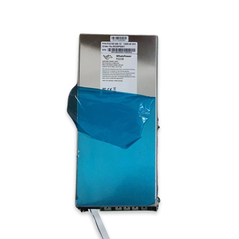
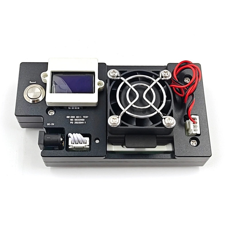
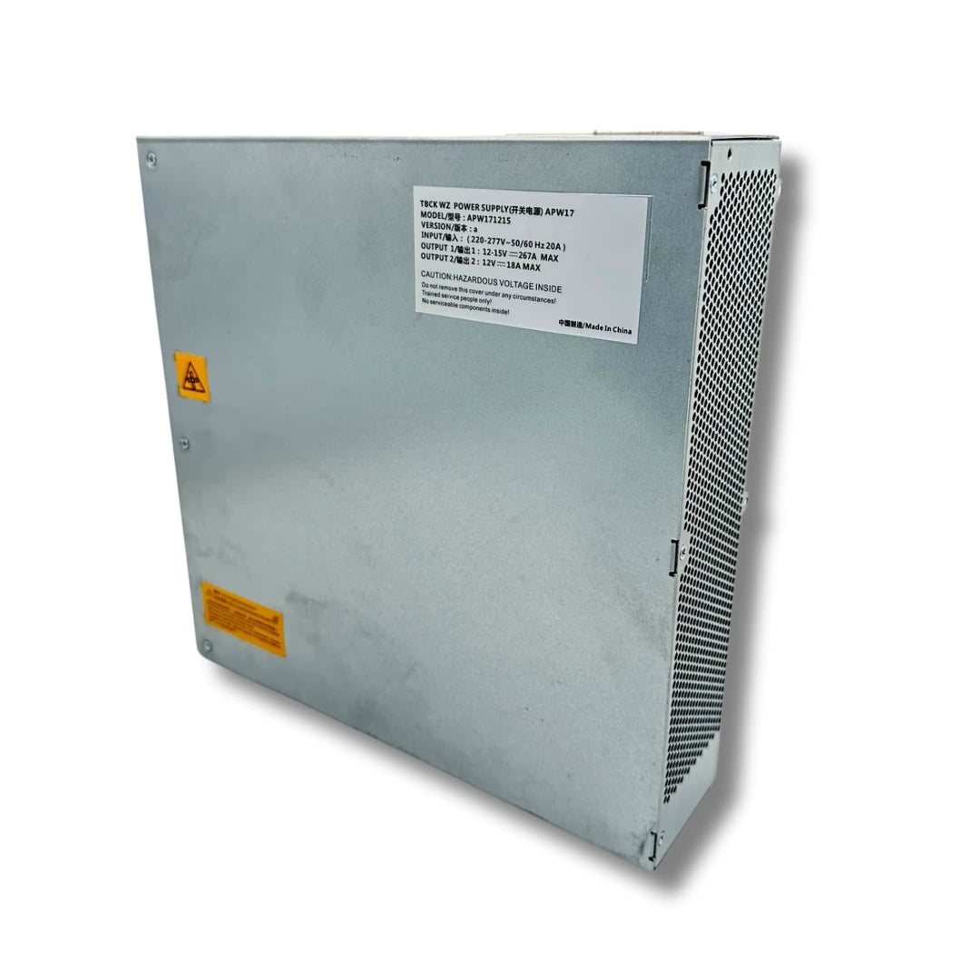
The D7 hashboard requires a V2.3 control board test fixture (Bitmain part number ZJ0001000001), powered by an APW12 1212V-15V V1.2 PSU with thick (4 AWG, <60cm) positive/negative copper cables. The test fixture's positive/negative terminals should be installed with discharge resistors — cement resistor 20Ω / 100W+. First use requires an SD card flash update of the V19-series test fixture FPGA. Standard test conditions: PT1 single-side detection (no scan code needed) and PT2 double-side 8× Pattern test (requires code scanner + RS232-to-TTL 3.3V serial adapter + network cable).
Most Common D7 Hashboard Failure Modes
- Zero chips detected (PT1/PT2 station, ASIC NG: 0) — the most common D7 fault. Use the dichotomy test method: short-circuit the RX test point and 1V8 test point between chips 1 and 2; check log. If still zero chips, check that 1V8 and 0V8 test points read 1.8V and 0.8V respectively. Most cases trace to short-circuit on the 0.8V or 1.8V SMD filter capacitors, or to the U1 / U2 / U5 circuits being poorly soldered, or to the first chip's pins not being properly tinned.
- Missing chips (specific count, ASIC NG: N) — use binary-search dichotomy. Short-circuit 1V8 and RO between chips 38 and 39; if log shows 38 chips, the first 38 are healthy. Continue halving the suspect range until the bad chip is isolated. When chip N is bad, shorting between chips N-1 and N shows the log finding N-1 chips, but shorting between N and N+1 still shows zero — that confirms chip N is the failure.
- ASIC 69 (one chip short, frequency 500MHz) — hashboard detects 69 of 70 chips. Use dichotomy to find the bad chip position, then verify and replace.
- EEPROM NG on test fixture LCD — check U10 (FM24C02B EEPROM) for solder integrity. Often a re-flow resolves; otherwise replace the FM24C02B EEPROM.
- PIC sensor NG on test fixture LCD — temperature reading abnormal. Check 4 resistors R214 / R215 / R1071 / R1076 for solder defects. Then check U5 / U7 / U8 / U9 S75 temperature sensor chips and their 3.3V supply. The heatsink-to-chip thermal interface deformation can also produce temperature anomalies and cascade-trip the sensor logic.
- Boost circuit 20V missing — measure C69 = 20V. If absent, check the TPHR9003NL primary MOSFET, the MP1517DR switching regulator IC, the boost inductor, the SY7302ABC DC-DC converter, and the surrounding small-signal MOSFETs (2N7002, MDU3603).
- U1/U2 burned after power-on — almost always indicates wrong power-on sequence (signal cable inserted before positive copper). U1 / U2 level converters (74AUP1T34 / NLSV1T34DFT2G / SN74LVC1G126DCKR) are sensitive to the power-on transient if signal voltage arrives before the rail is established.
- PIC microcontroller not responding (U6 pin 11 ≠ 3.3V) — verify the test fixture cable connection first. If cable is OK, reprogram the PIC16F1704 microcontroller using a PICkit3.5 programmer connecting to J3 pins 1-6. Burn the D7-specific HEX file via MPLAB IPE: select PIC16F1704 → Power → Operate → file select → Connect → Program → Verify.
- LDO output voltage out of spec — degraded SGM2036-1.8 or SGM2036-ADJ LDO chips. The MP2019GN low-current adjustable LDO can also drift on aged boards.
- Domain voltage low or open — typical domain voltage is about 0.3V. If 13V is supplied but no domain voltage, check MOS short-circuit (measure pins 1, 4, 8). Then check the BM1764 ASIC pair in that domain for short-circuit on the 0.8V or 1.8V filter capacitors.
- PCB temperature above 90°C — D7 monitoring alarms above 90°C. Causes: ambient too high (rated 20-30°C for PT2 testing; software stops above 35°C); fan abnormal; thermal compound degraded under the heatsink.
- Hashrate drop after assembly (boards OK in test fixture) — fit a healthy board with the test fixture in debug mode, set fan to 100%, adjust voltage/frequency to miner working values, monitor for hashrate loss. If still drops, lower frequency to 400M for diagnostic; remove heatsink and measure domain voltages live. Loss-of-hashrate with anomalous domain voltage usually means a chip is short-circuited or pin-tinning damaged on a specific chip.
D7 Hashboard Repair Components List
The table below lists every component LYS Shenzhen stocks for D7 hashboard repair. Each entry links directly to the corresponding part page — contact us at contact@lys-sz.com for bulk pricing or for the BM1764 ASIC chip itself (available by quote due to demand variability).
| Part Number | Component Type | Typical Position / Role |
|---|---|---|
| VS3510AP | P-channel MOSFET | D7 power switching (board-specific) |
| B0540W SF | Schottky diode | 40V / 500mA surface-mount auxiliary rectification |
| T2N7002AK NJ | N-channel MOSFET | Small-signal switching (shared with Antminer L7) |
| S75 | Temperature sensor | U5 / U7 / U8 / U9 positions — hashboard thermal monitoring |
| 330µF 6240k tantalum | Polymer tantalum capacitor | 2R5TPE330MCC2-1 — low-ESR domain decoupling |
| TPHR9003NL | N-channel MOSFET | 30V / 220A, 8-pin SOP — boost circuit primary switching |
| MBR230LSFT1G L3NE | Schottky diode | Power rectifier — cryptominer common |
| MP1517DR (LF-Z) | Switching regulator IC | QFN16, positive adjustable 3.3V output — auxiliary rail |
| 74AUP1T34 | Translating buffer | High-performance low-power dual-supply level translator |
| NLSV1T34DFT2G | Level translator | 1-bit dual-supply non-inverting — U1 / U3 / U4 positions |
| FM24C02B | I²C EEPROM | U10 position — hashboard ID / calibration storage |
| SMBJ190A PA | TVS diode | 190V transient suppression (shared L7 / D7) |
| BM1764 (stencil + chip replacement) | X11 ASIC chip + BM1764AB stencil | 70 chips per board × 35 domains × 2 chips. ASIC chip stocked by quote; BM1764AB stencil for chip replacement linked |
| SGM2036-1.8YN5G/TR | LDO regulator | 1.8V low-power LDO — domain rail generation |
| SGM2036-ADJYN5G/TR | LDO regulator | Adjustable, 0.8V typical output — domain decoupling chain |
| SN74LVC1G126DCKR (CN5/CNF) | Signal voltage conversion | Single-bit bus buffer — signal level conversion |
| 25.000 MHz crystal oscillator | Crystal oscillator | Y2 — generates the CLK (XIN) signal at chip 01 (voltage ~0.9V) |
| 330µF 30V SMD | Electrolytic capacitor | Domain rail decoupling |
| MBR0540 / MBR0540S / B4 | Schottky diode | Power rectifier — auxiliary stage |
| 10µH (Inductor 100) | Power inductor | Boost circuit / LDO output filtering |
| 2N7002-7-F | N-channel MOSFET | Small-signal switching |
| MDU3603 | N-channel MOSFET | Power switching (shared S17 / T17) |
| MP2019GN | LDO regulator | Adjustable low-current output |
| 47µF 50V SMD | Electrolytic capacitor | Auxiliary rail bulk filtering |
| SY7302ABC HMBWA | DC-DC converter | Power management IC — auxiliary stage |
| PIC16F1704-I/SLC01 | Microcontroller | U6 — 8-bit, 7KB flash, 14-pin — hashboard supervision + temperature reading + EEPROM bridge |
Diagnostic and Repair Workflow — 6-Step Bitmain-Documented Procedure
Bench setup requirements
- Anti-static maintenance workbench: grounded, anti-static wrist strap with grounding.
- Constant-temperature soldering iron: 350-380°C with pointed tip for chip resistors / capacitors.
- Hot air gun + BGA rework station: for chip / BGA disassembly and welding.
- Multimeter: Fluke 15B+ recommended, fitted with welded steel pins and heat-shrink sleeves for easy measurement.
- Oscilloscope: UTD2102CEX+ recommended.
- Network cable: stable internet connection for control-board test mode.
- APW12 PSU: AP12_12V-15V V1.2 + power adapter cable (4 AWG copper, <60cm length) for hashboard power.
- V2.3 control board test fixture: P/N ZJ0001000001 with 20Ω / 100W+ cement discharge resistors on positive/negative terminals.
- Serial port code scanner + RS232-to-TTL 3.3V adapter board for PT2 scan-code mode.
- Self-made short-circuit probe: pins welded onto wiring with heat-shrink sleeve to prevent shorts with small heatsinks (used in the dichotomy test method).
- Auxiliary materials: Solder paste 138°C, flux, Mechanic lead-free PCB cleaner, anhydrous alcohol, thermal conductive gel, ball-planting stainless steel mesh, desoldering wick, solder balls (0.4mm diameter recommended).
- Spare materials baseline: 0402 resistors (0R, 51R, 10K, 4.7K), 0402 capacitors (0.1µF, 1µF).
Safety and process discipline
The D7 hashboard repair procedure is unforgiving of mistakes. Three rules cannot be broken:
- Power-on sequence: negative copper cord first → positive copper cord second → signal cable last. Power-off sequence is the reverse: signal cable first → positive copper cord second → negative copper cord last. Wrong order destroys U1 / U2 level converters (and not always traceable to a specific chip).
- Cool-down before retest: after any rework, wait for the hashboard to cool completely before reapplying power for retest. Hot retest produces false PNG results.
- Heatsink + thermal gel before functional test: never run a chip-replacement validation without the large heatsink installed with fresh thermal-conductive gel applied evenly. Single-side production tests must form an air duct (place 2 hashboards side-by-side or use the chassis with 4 fans at full speed).
6-step diagnostic procedure
- Step 1 — Power output check. Verify the PSU is supplying 13V to the hashboard at the input terminals.
- Step 2 — Voltage domain output check. Each voltage domain should read about 0.3V at the chip pair. Priority is the hashboard's PSU input terminal and MOS short-circuit check (measure resistance between pins 1, 4, 8). If 13V is supplied but no domain voltage appears, continue.
- Step 3 — PIC circuit check. Measure U6 pin 11 = 3.3V output. If absent, verify the test fixture cable connection first. If cable is OK, reprogram the PIC16F1704 using a PICkit3.5 programmer on J3 pins 1-6. Burn the D7-specific HEX file via MPLAB IPE (select PIC16F1704 → Power → Operate → file select → Connect → Program → Verify).
- Step 4 — Boost circuit output check. Test point C69 = 20V (output of U238 boost). If absent, work back through TPHR9003NL primary MOSFET, MP1517DR switching regulator, boost inductor, and surrounding small-signal MOSFETs.
- Step 5 — LDO output check. Verify 1.8V LDO output (each domain) and 0.8V PLL output (each domain). Check the SGM2036-1.8 and SGM2036-ADJ LDOs in sequence — these are the most common drift points on aged boards.
- Step 6 — Chip signal output check. Trace CLK / CI / RO / BI / RST signals. Reference voltage values: CLK ~0.9V; RST + CI from J3 pin 3 (3.3V) post-level-conversion. If measured values differ significantly from reference, compare with adjacent domain measurements. When dichotomy method localises a bad chip, re-solder the chip first (add no-clean flux, heat solder joints to dissolved state, promote re-tinning) before replacing — the issue may be poor solder contact rather than a dead chip.
Dichotomy method — chip-level localisation
Bitmain's dichotomy (binary-search) test method is the fastest path to localise a missing chip on a D7 hashboard:
- If LCD reports ASIC NG: 0 (zero chips) — short-circuit RX test point and 1V8 test point between chips 1 and 2 with the self-made short-circuit probe. Run program and check serial log. If still 0 chips: most likely cause is 0.8V / 1.8V SMD filter cap short, U1 / U2 / U5 poor soldering, or chip 1 pin tinning failure.
- If first attempt finds 1 chip — first chip and previous circuit are healthy. Halve the remaining range and short-circuit 1V8 + RO between chips 38 and 39. If log shows 38 chips, first 38 are healthy. If still 0, the fault is in chips after 38. Continue halving until isolated.
- If log shows ASIC 69 (one chip short, frequency 500MHz) — use dichotomy to find the bad chip position. Re-test the same chip first; if result is identical, the chip is bad and needs replacement.
- If chip N is bad, then shorting between N-1 and N finds N-1 chips, but shorting between N and N+1 still finds 0 — this confirms the position. Optional sanity check: swap chip N and N+1; if shorting between N-1 and N now finds N-2 chips (one off because N is now at position N+1), the chip is confirmed bad.
Test fixture report codes and post-repair validation
- ASIC NG: 0 — zero chips detected. Apply dichotomy method.
- ASIC NG: N — N chips detected (where N < 70). Apply dichotomy method to localise.
- ASIC 69 — 69 chips at 500MHz frequency. Localise the missing chip and verify before replacing.
- EEPROM NG — check U10 FM24C02B EEPROM solder integrity; re-flow or replace.
- PIC sensor NG — temperature read abnormal. Check R214 / R215 / R1071 / R1076; check U5 / U7 / U8 / U9 S75 temperature sensors + their 3.3V supply; check heatsink-to-chip thermal interface for deformation.
- PLUG OFF BEFORE TEST OVER — software delay during shutdown; tester unplugged cable too early. Restart fixture.
PT2 test environment requirements
- Ambient temperature: 20-30°C. Above 35°C the test software stops automatically.
- PSU output stability under load: at 1500W load, the PSU output cannot drop more than 0.03V below the configuration-file value (e.g. 15V configured → actual output ≥14.97V at 1500W).
- Post-repair validation: hashboard must pass test fixture validation more than twice to be cleared. First pass after rework, then a second pass after the board has cooled completely. After test pass, remove the large heatsink, brush fresh thermal-conductive gel, install the heatsink, and run through the production-line first station including PT1 and PT2.
- Whole-miner aging test: install repaired hashboard into a complete miner for at least one aging cycle. Monitor for fan abnormality, chain detection, temperature alarms above 90°C, hashrate drop after assembly.
Whole Miner Failure Diagnosis
D7 whole-miner faults are usually traceable to the test fixture results above. The most common assembly-level faults:
- IP not detected — check ARM/CPU appearance, network port T1 transformer, control board PIC. If single board passes PT2 but whole miner fails, the issue is usually the control board (7007 board) or the cable connection.
- Chain missing / fewer boards detected — usually a cable connection issue. Check the cable for open circuit; test the suspect board on PT2; if it passes, the control board chain is the problem.
- Abnormal temperature (PCB >90°C) — alarm threshold. Most common cause: ambient too high, fan abnormal, or thermal compound degraded.
- Hashrate drop after assembly (boards OK in test fixture) — fit a healthy board with test fixture in Debug master chip program, set fan to 100%, adjust voltage/frequency to miner working values, monitor for hashrate loss. If still drops, lower frequency to 400M for diagnostic; remove heatsink and measure domain voltages live. Anomalous domain voltage usually means a chip is short-circuited or pin-tinning damaged on a specific chip.
- Control board OTP failure (7007 board) — wait 30 seconds after card-flash for OTP to complete. Power failure before OTP completes burns the U1 main control IC (FBGA package), which is irrecoverable on D7 series — U1 cannot be reused on D7 after OTP failure.
When Chip-Level Repair Makes More Sense Than Replacement
New D7 hashboard stock is constrained — Bitmain stopped volume manufacturing this generation years ago, and the secondary market is mostly other operators' failed boards. For Dash mining operators, component-level repair is the realistic path. A small inventory of the BM1764 ASIC chips (the most-replaced part), the boost circuit MOSFETs (TPHR9003NL, MDU3603), the LDO chain (SGM2036-1.8, SGM2036-ADJ, MP2019GN), the level translators (74AUP1T34, NLSV1T34DFT2G, SN74LVC1G126DCKR), the PIC16F1704 microcontroller (with the D7 HEX file ready to flash), the S75 temperature sensors, and the small-signal MOSFETs (2N7002, T2N7002AK) covers the majority of bench-repair scenarios.
Several D7 components are shared across other Bitmain miners — T2N7002AK with the Antminer L7, MDU3603 with the S17 / T17, MP2019GN with the S17 / S19, SN74LVC1G126DCKR with the S19 family, MP1517DR with the S17 / T17 / S19 / T19, and PIC16F1704 with the broader Antminer hashboard line. A repair bench that already stocks parts for one Bitmain generation can extend coverage to the D7 with relatively few additions.
FAQ — Antminer D7 Hashboard Repair
What is the hashboard layout on the Antminer D7?
The D7 hashboard (BXD34601) carries 70 BM1764 ASIC chips arranged in 35 voltage domains × 2 chips per domain. The whole D7 miner has 3 hashboards (210 chips total) + 1 control board + 1 APW12 PSU + 4 cooling fans. Each chip operates at ~0.3V domain voltage; the boost circuit U238 supplies 20V from the 13V PSU input.
What is the test fixture for D7 repair?
D7 hashboards use a V2.3 control board test fixture (Bitmain P/N ZJ0001000001), powered by an APW12 1212V-15V V1.2 PSU with 4 AWG copper cables (<60cm length) and 20Ω / 100W+ cement discharge resistors on the test rig terminals. PT1 mode does not require scan codes; PT2 mode requires a serial port code scanner and RS232-to-TTL 3.3V adapter board with network cable. First use requires an SD-card firmware update for the V19-series test fixture FPGA.
What is the correct power-on sequence for D7 hashboard repair?
Negative copper cord first → positive copper cord second → signal cable last. Power-off is the reverse: signal cable first → positive copper cord → negative copper cord. Wrong order destroys U1 / U2 level converters and is not always traceable to a specific chip — this is the most common bench-error cause of D7 hashboard failure after repair.
How do I localise a bad chip on the D7 hashboard?
Use the dichotomy (binary-search) test method with a short-circuit probe. Short-circuit RX + 1V8 test points between chips 1 and 2 first; if 0 chips report, the fault is in the first chip or its surrounding U1/U2/U5 circuit or filter capacitors. If 1 chip reports, halve the remaining range — short between chips 38 and 39; if 38 chips report, the first 38 are healthy. Continue halving until the bad chip is isolated. When chip N is bad, shorting between N-1 and N finds N-1 chips, but shorting between N and N+1 finds 0.
What does ASIC 69 mean on the D7 test fixture LCD?
The hashboard detects 69 of 70 chips at 500MHz test frequency. One chip is missing. Use the dichotomy method to find the position. Re-test the same chip first (sometimes a marginal contact restores between tests); if the same chip remains bad, it needs replacement. Re-solder the chip with no-clean flux first — sometimes the issue is poor solder contact rather than a dead chip.
How do I reprogram the PIC16F1704 on a D7 hashboard?
Use a PICkit3.5 programmer connected to J3 pins 1-6 (pin 1 of PICkit3 cable matches pin 1 of J3 on PCB). Open MPLAB IPE; select PIC16F1704 as device; click Power to select power method then click Operate; Select File to find the D7-specific HEX file; click Connect; click Program; on completion click Verify. A "verification complete" message confirms the burn succeeded.
Is the D7 still profitable to repair in 2026?
D7 economics are tight in 2026 — block reward and Dash mining margin have compressed. The path depends on electricity cost: in cheap-power regions, a healthy D7 fleet can earn for another 2-3 years with structured maintenance and parts inventory. New D7 hashboards are scarce; component-level repair on the existing fleet is the realistic path for most operators. Contact LYS Shenzhen at contact@lys-sz.com for parts pricing and bulk supply.
Sourcing D7 Hashboard Repair Parts
LYS Shenzhen stocks every component listed above for the Antminer D7 hashboard. The BM1764 ASIC chip itself is stocked by quote (demand variability — please email with quantity). For the BM1764AB tin-tool stencil for chip replacement, see the linked product page. For the broader Antminer altcoin lineup (L7 Scrypt, L9 Scrypt), or for D7 complete-miner sourcing, contact our team at contact@lys-sz.com — we operate an on-demand sourcing channel for repair components across the full Bitmain altcoin miner range.
Worldwide shipping from our Shenzhen warehouse via DHL, FedEx, UPS, and sea freight. DDP shipping available for US and EU customers; case-by-case for other lanes — request a quote with your shipping country for confirmation.