Antminer ASIC Chips — Complete Reference & Hashboard Repair Guide (2026 Update)
An ASIC (Application-Specific Integrated Circuit) is a chip built for one task only — in Bitcoin mining, computing SHA-256 double hashes as fast and efficiently as physically possible. Since Bitmain shipped the first 55nm BM1380 chip on the Antminer S1 in late 2013, the ASIC silicon inside each Antminer generation has driven the entire economic and security trajectory of the Bitcoin network. This guide is the comprehensive 2026 reference to every Bitmain Antminer ASIC chip ever released, paired with the hashboard model it powers, the process node it was fabricated on, the chip count per board (where known), and the LYS Phase 2 repair-chip SKU that drops in as a direct replacement. Updated to include the latest BM1368 (S21 / T21 / S21 Hydro), BM1370 (S21 Pro / S21 XP / S21+ Plus Hydro), and BM1373CC (S23 Hydro) generations missing from the original 2023 BOM list.
Why ASIC Chip Identification Matters for Repair
Every Antminer hashboard is built around dozens of ASIC chips arranged in a serial daisy chain — each chip receives data from the previous chip and passes results to the next. A single dead chip in the chain takes the entire chain offline, regardless of how many other chips are healthy. This is why bench repair starts with chip identification: knowing which BM-series chip your specific Antminer model uses tells you (a) which stencil + reballing kit to source for chip replacement, (b) which donor boards can be harvested for compatible chips, and (c) which repair-bench inventory items are cross-shared with adjacent miner generations.
The repair economics depend on accurate chip mapping. Sourcing a BM1366AG when you actually need a BM1366BS (both 5nm chips, both labelled "BM1366 family", but the AG variant is the S19 XP chip and the BS variant is the S19K Pro chip) results in a wasted bench session and a chip that won't pair-bond with the rest of the chain. The comprehensive chip table below disambiguates every BM-series variant against its exact Antminer model.
The Six Eras of Antminer ASIC Chips
Bitmain's chip development progressed through six identifiable generations from 2013 to 2026. Each generation represents a process-node shrink and/or architectural revision that delivered meaningful efficiency gains:
| Era | Process Node | Period | Representative Chip | Representative Miner | Efficiency (J/TH) |
|---|---|---|---|---|---|
| Gen 1 — Concept proof | 55nm / 28nm | 2013-2015 | BM1380 / BM1384 / BM1385 | S1 / S5 / S7 | ~2000-1500 |
| Gen 2 — S9 mass deployment | 16nm | 2016-2019 | BM1387 | S9 / S9i / S9j / L3+ | ~98 |
| Gen 3 — S17 era | 7nm | 2019-2020 | BM1397 / BM1391 / BM1396 | S17 / T17 / S15 | ~40-50 |
| Gen 4 — S19 workhorse | 7nm refined | 2020-2023 | BM1398 / BM1362 | S19 / S19j Pro / S19j Pro+ | ~29-32 |
| Gen 5 — 5nm shrink | 5nm | 2022-2024 | BM1366 family | S19 XP / S19K Pro | ~21.5 |
| Gen 6 — S21 / S23 latest | 5nm refined / 3nm | 2024-2026 | BM1368 / BM1370 / BM1373CC | S21 / T21 / S21 Pro / S21 XP / S23 Hydro | ~13.5-17.5 |
The headline number to grasp: the BM1380 (S1, 2013) operated at roughly 2000 J/TH; the BM1370 (S21 Pro, 2024) operates at ~17.5 J/TH. That is more than 100× improvement in energy efficiency over 11 years — driven by process-node shrinks from 55nm down to 5nm and architectural refinement of the SHA-256 hashing cores.
Modern Antminer ASIC Chip Map (2024-2026 Generations)
The most operationally relevant chips for 2026 repair work are the Gen 4 / 5 / 6 generations. These are the chips on the hashboards that operators are actively maintaining and repairing today:
S19 family (BM1398 + BM1362 — 7nm)
- BM1398 family (BM1398BB / BM1398AC / BM1398AD) — the workhorse 7nm S19 chip. BM1398BB powers the standard S19 (~76-114 chips per board × 3 boards), BM1398AC powers the S19+ / S19a Pro, BM1398AD powers the S19a / S19a Pro variants. Currently one of the most-repaired chips in active queues — the S19 generation is the largest installed BTC mining fleet in 2026.
- BM1362AJ — paired with S19j / S19j Pro. The BM1362AA / BM1362AC / BM1362AI variants share the same family. Critical BHB part numbers: BHB42801 (S19j Pro 126 chips × 42 domains × 3 chips per domain) and BHB42831 (S19j Pro+ with BM1362AK — 88 chips × 44 domains × 2 chips per domain).
- BM1362AK — specific to BHB42831 PCB revision of the S19j Pro+. 88 chips × 44 domains × 2 chips per domain.
- BM1362BD — dedicated S19j Pro+ (Plus) variant. 120 chips × 40 domains × 3 chips per domain. Distinct from the S19j Pro's BM1362AJ/AK.
- BM1398BB (Hydro) — S19 Hydro HHB28601 hashboard: 104 BM1398BB chips × 52 domains × 2 chips per domain. Dual-oscillator architecture (Y1 / Y2 split — BM1-51 vs BM52-104) distinct from air-cooled S19.
5nm Generation (BM1366 family)
- BM1366AL / BM1366AG — S19 XP / S19 XP Hydro. The original LYS BOM list noted "BM1366AL/AG S19XP / S19XP Hydro". BHB56801 hashboard carries 110 BM1366AG chips × 11 domains × 10 chips × 3 boards = 330 chips total. 141 TH/s at 21.5 J/TH — the first Antminer at sub-30 J/TH efficiency.
- BM1366BS / BM1366BP — S19K Pro. BHB56902 hashboard, ~328 chips total at 110-120 TH/s. The BM1366 family covers both S19 XP and S19K Pro — different revision suffixes (AL/AG vs BS/BP) signal different production runs and binning.
S21 / T21 / S21 IMM / S21 Hydro / S21e XP Hyd 3U (BM1368 — 5nm refined) — NEWLY ADDED 2024 GENERATION
-
BM1368AA + BM1368PB — current production for the entire S21 family. PA / PB / PV / PM / AA suffix variants signal production binning. Cross-compat across S21 / T21 / S21 IMM / S21 Hydro per the LYS product URL naming. Reference deployments:
- BHB68XXX air-cooled hashboard = 108 BM1368 chips × 12 domains × 9 chips per domain (S21 / T21). 200 TH/s at 17.5 J/TH.
- HHB68xxx hydro hashboard = 216 BM1368 chips × 18 domains × 12 chips per domain (S21 Hydro — 2× the chip density of air-cooled).
- Antminer S21e XP Hyd 3U — high-end enterprise-tier 830-860 TH/s, 380V AC input, hydro-cooled 3U form factor. Also powered by the BM1368 family — same chip generation, scaled with higher chip count per chassis.
S21 Pro / S21 XP / S21+ Plus / S21e XP Hydro (BM1370 — 5nm refined) — NEWLY ADDED 2024-2026 GENERATION
-
BM1370 family — variants BB / BC / AA / PA / PB — current production for the higher-tier S21 lineup. BM1370 is a refinement of the 5nm BM1368 architecture with tighter ball pitch and improved per-chip efficiency. Powers:
- Antminer S21 Pro (~234 TH/s at 15 J/TH; 216 chips per hashboard per industry references)
- Antminer S21 XP (~270 TH/s at 13.5 J/TH — the efficiency leader of the standard S21 generation)
- Antminer S21+ (Plus) Hydro — water-cooled higher-density variant, 216 BM1370 chips per board
- Antminer S21e XP Hydro — enterprise-tier hydro variant at 13 J/TH, direct liquid-to-chip cooling for peak efficiency
- Bitaxe 601 Gamma (open-source home solo miner) — same BM1370 silicon as the Antminer S21 Pro, in an open-source hardware design. Same industrial chip, retail-accessible form factor — the decentralization angle of having identical silicon on industrial and home miners.
S23 Air / Hydro / IMM (BM1373CC — 3nm) — NEWLY ADDED 2025-2026 GENERATION
-
BM1373CC — the latest Bitmain chip on the 3nm process node. Single-chip hashrate ~400-500 GH/s per industry references (vs ~200 GH/s on the previous BM1370 generation = ~2× per-chip improvement). The S23 line spans three variants:
- Antminer S23 Air — ~318 TH/s at the air-cooled efficiency point
- Antminer S23 Hydro — hydro-cooled enterprise variant, ~127 BM1373CC chips per hashboard per industry references
- Antminer S23 IMM — immersion-cooled variant for hyperscale farm deployments
Comprehensive Antminer ASIC Chip Table (Including Older + Niche Generations)
The table below covers every Bitmain Antminer ASIC chip ever released, including older generations still in repair queues, altcoin-algorithm chips (L7 Scrypt, D7 X11, K-series KAS), and niche / regional variants. Where LYS stocks the chip as a direct replacement, the product page is linked. Where LYS stocks the chip stencil / tin tool for chip replacement (but not the chip itself, which is typically by-quote), the tin tool is linked.
| ASIC Chip Variant | Antminer Model(s) | Algorithm / Notes |
|---|---|---|
| Gen 1 — Early SHA-256 generations (2013-2015) | ||
| BM1380 (55nm) | S1 — original Antminer (2013) | SHA-256 — historic first ASIC; mostly retired |
| BM1384 | S5 | SHA-256 — retired |
| BM1385 | S7 | SHA-256 — retired but still occasionally found |
| Gen 2 — S9 / L3 era (16nm, 2016-2019) | ||
| BM1387B / BM1387BL | S9 / S9i / R4 / T9+ | SHA-256 — the most-deployed Bitmain ASIC in history (~98 J/GH = ~0.098 J/TH-equivalent). Many S9s still operating as space heaters. |
| BM1387BE | S9J / T9J | SHA-256 — S9J production variant |
| BM1387BF | S11 / S9J / T9J | SHA-256 — late S9-era production |
| BM1393B | S9K | SHA-256 — S9K refresh variant |
| BM1393CE (BM1393CE_BGM) | S9 SE | SHA-256 — S9 SE special edition |
| BM1485 | L3 / L3+ / L3++ | Scrypt (Litecoin / Dogecoin merged mining) — predecessor to BM1489 |
| BM1487AA | L5 | Scrypt — L5 variant |
| Gen 3 — S17 / S15 era (7nm, 2019-2020) | ||
| BM1391AE | S15 / T15 | SHA-256 — first 7nm Bitmain chip generation |
| BM1396AB | S17e / T17e | SHA-256 — efficiency variant |
| BM1397AD / AG / AH / AI / AF | S17 / S17+ / S17 Pro / T17 / T17+ | SHA-256 — S17 generation workhorse; D-Central documents this generation as having particularly high BGA-cracking failure rate due to thermal cycling on lead-free solder |
| Gen 4 — S19 workhorse (7nm refined, 2020-2023) | ||
| BM1398BB | S19 / S19 Pro / T19 | SHA-256 — S19 standard. 76 chips × 3 boards (most production revisions) |
| BM1398AC | S19+ / S19a / S19a Pro | SHA-256 — S19 variant family |
| BM1398AD | S19a / S19a Pro | SHA-256 — alternative production variant |
| BM1398BB (Hydro) | S19 Hydro (HHB28601) | SHA-256 — 104 chips × 52 domains × 2 chips per domain. Dual oscillator Y1 / Y2 split. |
| BM1360BB | S19i / S19j Pro variant | SHA-256 — niche production variant |
| BM1362AA / BM1362AC / BM1362AI / BM1362AJ | S19j / S19j Pro | SHA-256 — S19j Pro standard. 126 chips × 42 domains × 3 chips per domain (BHB42801 PCB rev) |
| BM1362AK | S19j Pro / S19 Hydro (BHB42831 PCB rev) | SHA-256 — 88 chips × 44 domains × 2 chips per domain (specific to BHB42831 production revision) |
| BM1362BD | S19j Pro+ (Plus) | SHA-256 — S19j Pro+ dedicated variant. 120 chips × 40 domains × 3 chips per domain |
| Gen 5 — 5nm shrink (BM1366 family, 2022-2024) | ||
| BM1366AL / BM1366AG | S19 XP / S19 XP Hydro | SHA-256 — 5nm. BHB56801 hashboard 110 chips × 11 domains × 10 chips × 3 boards = 330 total. 141 TH/s at 21.5 J/TH. |
| BM1366BS / BM1366BP | S19K Pro | SHA-256 — 5nm. BHB56902 hashboard, ~328 chips total at 110-120 TH/s. |
| Gen 6 — S21 / S23 latest (5nm refined / 3nm, 2024-2026) | ||
| BM1368AA + BM1368PB (PA/PB/PV/PM/AA variants) | S21 / T21 / S21 IMM / S21 Hydro / S21e XP Hyd 3U | SHA-256 — 5nm refined. S21 air = 200 TH/s at 17.5 J/TH (108 chips × 12 × 9). S21 Hydro = 216 chips × 18 × 12 (2× density). S21e XP Hyd 3U enterprise variant = 830-860 TH/s at 380V AC input. |
| BM1370 family (BB / BC / AA / PA / PB variants) | S21 Pro / S21 XP / S21+ (Plus) Hydro / S21e XP Hydro / Bitaxe 601 Gamma (open-source home miner) | SHA-256 — 5nm refined. S21 Pro ~234 TH/s at 15 J/TH (216 chips); S21 XP ~270 TH/s at 13.5 J/TH; S21e XP Hydro at 13 J/TH (direct liquid-to-chip cooling, efficiency leader). Finest ball pitch in Antminer lineup — pro-only rework. Same silicon also used in Bitaxe Gamma open-source home miner — industrial chip in retail form factor. |
| BM1373CC | Antminer S23 Air / S23 Hydro / S23 IMM | SHA-256 — 3nm process node. Single-chip hashrate ~400-500 GH/s (~2× per-chip vs BM1370). S23 Air ~318 TH/s; S23 Hydro ~127 chips per board. The first Antminer below 13 J/TH at production scale. Also deployed in third-party "NEXUS S1" desktop solo miner. |
| Altcoin algorithms (Scrypt / X11 / KAS / etc.) | ||
| BM1489 (also "B20") | L7 | Scrypt (Litecoin / Dogecoin) — 120 chips × 24 voltage domains × 5 chips per domain |
| BM1764 | D7 | X11 (Dash) — 70 chips × 35 voltage domains × 2 chips per domain |
| BM2042AA | K7 | KAS (Kaspa kHeavyHash) — Antminer K-series KAS miner |
| BM2280AA | K7 | KAS — K7 alternative production variant |
| BM2110AA | KA3 | KAS — Antminer KA3 KAS miner |
| BM1798AA | E9 | EThash (Ethereum / Ethereum Classic) — pre-PoS migration |
| BM1720 | A3 | Blake (256) — alt algorithm |
| BM1760 | D3 | X11 (Dash) — predecessor to D7's BM1764 |
| BM1725AA | DR5 | Blake (256R14) — Decred |
| BM1762 | D5 | X11 — niche |
| BM1744AB / BM1744BB | Z11 / Z11j / Z11e | Equihash — Zcash |
| BM1746AA | Z15 | Equihash — Zcash newer variant |
| BM1840 | B7 | Tensority — Bytom |
| BM2040 | K5 | Eaglesong — Nervos CKB |
| BM1740 | Z9 mini / Z9 | Equihash — Zcash legacy |
| BM1722 | DR3 | Blake — Decred legacy |
| BM1700 | X3 | CryptoNight — Monero legacy |
| BM1680 | B3 | Tensority — Bytom legacy |
| BM1580L3 (BM1580) | V9 | SHA-256 — niche entry-tier |
| BM2130 | HS3 | Handshake |
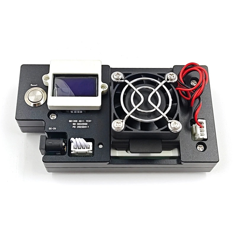
Hashboard Architecture: What the Chips Are Connected To
Knowing the chip is half the battle — the other half is understanding what the chip connects to on the hashboard. Every Antminer hashboard, regardless of generation, shares the same architectural elements:
- ASIC chip array: dozens of identical BM-series chips connected in a serial daisy chain. CK (clock) + RST (reset) + CI/CO (chain in/out for data) + BO (status) signal lines flow through the chain. A single dead chip kills the entire chain downstream.
- Voltage domains: ASIC chips operate at very low voltages (0.3-1.2V per domain depending on generation and frequency). The PSU supplies 12V (or higher for newer generations); the hashboard's buck converters step this down through multiple voltage domains, each powering a group of chips. A failed buck converter or shorted MOSFET in a voltage domain takes every chip in that domain offline.
- Signal chain coupling capacitors + termination resistors: couple signals between domains (different voltage references) and prevent reflections at chain ends.
- Temperature sensors: NTC thermistors at strategic locations across the board feed the control board's fan-speed regulation and thermal-shutdown logic.
- LDO regulators: provide clean PLL / I/O supply rails to the ASIC chips (separate from the main core voltage).
- EEPROM: stores board-specific calibration data (voltage trim, frequency tables). Corruption can cause erratic behaviour even when all hardware is functional.
For deep architectural dives per Antminer generation, see the dedicated hashboard repair guides:
- S19 standard, S19j / S19j Pro, S19j Pro+ (Plus), S19 XP, S19 Hydro HHB28601, S19K Pro
- S21 / T21, S21 Hydro
- L7 (Scrypt), D7 (X11)
Most Common ASIC Chip Failure Modes
- Dead ASIC chip (most common single-fault mode): a chip stops responding entirely. Symptoms: kernel log shows chain enumeration stopping at a specific chip number; board reports zero or reduced hashrate; ASIC status string shows "x" at the failed position. Causes: cumulative thermal stress, electromigration at nm-scale interconnects, manufacturing defects, voltage spikes.
- BGA solder joint failure / cracking: thermal cycling (heating + cooling cycles of normal operation) creates micro-cracks in the BGA solder balls connecting the chip to the PCB. Often intermittent — works cold, fails hot. The Antminer S17 / T17 generation (BM1397) is particularly notorious for this failure mode due to a combination of high operating temperatures and lead-free solder formulations. The newer 5nm + 3nm chips with tighter ball pitch are also vulnerable.
- Voltage domain failure: buck converter IC, MOSFETs, or output capacitors in a voltage domain fail. Every chip in that domain goes dark. Thermal imaging shows a distinct cold zone where the dead domain sits.
- Signal chain break: damaged PCB trace, failed coupling capacitor between voltage domains, or a single chip failure that takes downstream chips offline. Often presents as partial chain detection (e.g. 30 of 76 chips detected).
- Thermal damage: sustained operation above thermal envelope degrades every component progressively. Brown/dark PCB substrate + bubbled flux residue = visible thermal damage indicators.
- ESD damage: invisible. A static discharge below human perception threshold (under 100V) can destroy chip I/O structures. Most common in environments without proper anti-static wrist straps + grounded benches.
- Corrosion / moisture damage: humid mining environments (basements, garages) + airborne contaminants cause copper trace corrosion + connector pin oxidation. White/green crystalline deposits on PCB = moisture damage.
ASIC Chip Replacement: Professional vs DIY Threshold
Chip replacement requires BGA (Ball Grid Array) rework — there are no through-hole leads to desolder. The chip sits flat on the board with hundreds of tiny solder balls forming the connection underneath. Standard workflow:
- Apply flux around the chip; preheat the board from below to 150-180°C to reduce thermal shock.
- Heat the chip from above with a hot air rework station: 350-380°C for lead-free SAC305 solder; 300-330°C for leaded Sn63/Pb37.
- Lift the chip with vacuum tweezers when solder reflows. Never twist or pry — risk of lifting PCB pads.
- Clean pads with solder wick + flux + isopropyl alcohol. Inspect for lifted/damaged pads.
- Reball the replacement chip if needed (model-specific BGA stencil + jig + 0.4mm solder balls).
- Apply flux to PCB pads, align replacement chip, reflow with hot air. Inspect under magnification for bridges + misalignment.
The process takes 15-30 minutes per chip for an experienced technician. Newer chips (BM1366, BM1368, BM1370, BM1373CC) have finer ball pitch and demand greater precision + better equipment. The DIY-vs-professional threshold:
- DIY-friendly: visual inspection, basic multimeter testing (resistance + diode mode), firmware diagnostics (kernel logs + chip count + per-chip hashrate + error rates), fan and cable replacement, heatsink + thermal paste maintenance, control board swapping.
- Requires professional equipment: any BGA component removal/installation, buck converter + MOSFET replacement (high-current thermal-pad work), trace repair (microscope precision + signal integrity knowledge), BGA reballing (model-specific stencils + jig), multi-fault diagnosis.
The threshold is simple: if the repair requires removing or installing a BGA component, it requires professional equipment and skills. Everything up to that point is accessible to a careful, methodical operator willing to learn.
LYS Chip Stencils / Tin Tool Fixtures for Chip Replacement
LYS Shenzhen stocks model-specific BGA stencils + tin tool fixtures for chip replacement across the Antminer lineup. These are the dedicated tooling required to align the chip + reballing stencil + jig during the rework process:
- BM1397 / BM1387 / BM1485 4-in-1 universal tin tool fixture — covers S9 + S17 + L3 generation in a single fixture
- BM1398 / BM1398BB tin tool fixture with stencil and holder — S19 generation
- BM1362AA tin tool fixture — S19j / S19j Pro generation (100mm)
- BM1362AK tin tool fixture + holder — S19j Pro BHB42831 PCB revision
- BM1362AK stencil tin tool fixture — S19j hashboard chip stencil
- BM1764AB tin tool stencil — D7 hashboard chip replacement
- BM1489 tin tool fixture — L7 hashboard chip replacement
- BM2042AA precision tin tool fixture — Antminer K7 KAS hashboard
- BM2110AA tin tool stencil — Antminer KA3 KAS hashboard
FAQ — Antminer ASIC Chips
How do I identify which ASIC chip my Antminer uses?
Match your Antminer model number to the chip table above. The chips are physically printed with their part number on the package (e.g. "BM1398BB" or "BM1366AL"), so opening the hashboard and reading the chip silkscreen confirms the identifier. For S19j Pro generation, the PCB revision (BHB42801 vs BHB42831) determines which BM1362 sub-variant the board uses — 42801 = BM1362AJ; 42831 = BM1362AK.
What is the difference between BM1366AL/AG (S19 XP) and BM1366BS/BP (S19K Pro)?
Both are 5nm chips in the BM1366 family, but they are different sub-variants paired with different miners. BM1366AL / AG = S19 XP / S19 XP Hydro (BHB56801 hashboard, 141 TH/s). BM1366BS / BP = S19K Pro (BHB56902 hashboard, 110-120 TH/s). Cannot cross-substitute — the AG/AL variants will not pair-bond with the BS/BP chain on an S19K Pro board.
Which Antminer chips are most active in 2026 repair queues?
The S19 generation (BM1398BB + BM1362 family) accounts for the largest share of active repair work — most S19 units are 3-5 years into service, in the failure zone. The S17 generation (BM1397) is notorious for BGA cracking and continues to require rework. The new S21 generation (BM1368) is starting to enter repair queues as the early production cohort ages out of warranty.
What is the latest Antminer chip in 2026?
BM1373CC — fabricated on the 3nm process node, powering the Antminer S23 Hydro at the network's leading efficiency point. BM1370 (5nm refined, S21 Pro / S21 XP / S21+ Plus Hydro) is the most-deployed current-generation chip in 2026 with ~13.5-17.5 J/TH efficiency.
Can I repair an S9 hashboard with a BM1387 chip in 2026?
Yes — replacement BM1387 chips are still readily available and inexpensive. S9 hashboard repair is economically viable for operators running S9 fleets as Bitcoin space heaters where the heat output justifies the electricity cost regardless of pure mining profitability. For pure mining profitability, S9 boards are marginal at current difficulty.
Why does a single failed chip kill the entire hashboard chain?
ASIC chips on Antminer hashboards are connected in a serial daisy chain — each chip receives data from the previous chip and passes results to the next. When one chip dies, the data flow stops at that position. Every chip downstream of the failed chip is healthy but unreachable. This is why localising the FIRST failed chip in the chain (read the AUC3 `estats` ASIC status string for Avalon or the Antminer kernel log for Bitmain) is the critical diagnostic step.
Can I replace an ASIC chip myself?
Technically yes, but practically it requires a hot air rework station ($200-$1000+), BGA reballing equipment, model-specific stencils + jig, practice boards, and significant soldering skill. The newer 5nm + 3nm chips (BM1366, BM1368, BM1370, BM1373CC) have finer ball pitch and demand professional-grade equipment + experience for reliable results. Most home miners are better served by professional repair for BGA work; everything up to BGA work (visual inspection, multimeter testing, firmware diagnostics, fan/cable replacement) is DIY-friendly.
Sourcing Antminer ASIC Chips & Hashboard Repair Parts
LYS Shenzhen stocks the full Antminer ASIC chip lineup as direct replacements + model-specific BGA stencils + tin tool fixtures for chip rework. For the chips themselves (Gen 4 / Gen 5 / Gen 6 generations are stocked direct; older Gen 1-3 chips are typically by quote due to demand variability), contact our team at contact@lys-sz.com with your specific Antminer model + PCB revision (e.g. "S19j Pro BHB42831" = BM1362AK; "S19 XP BHB56801" = BM1366AG).
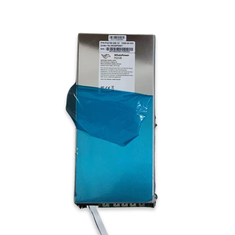
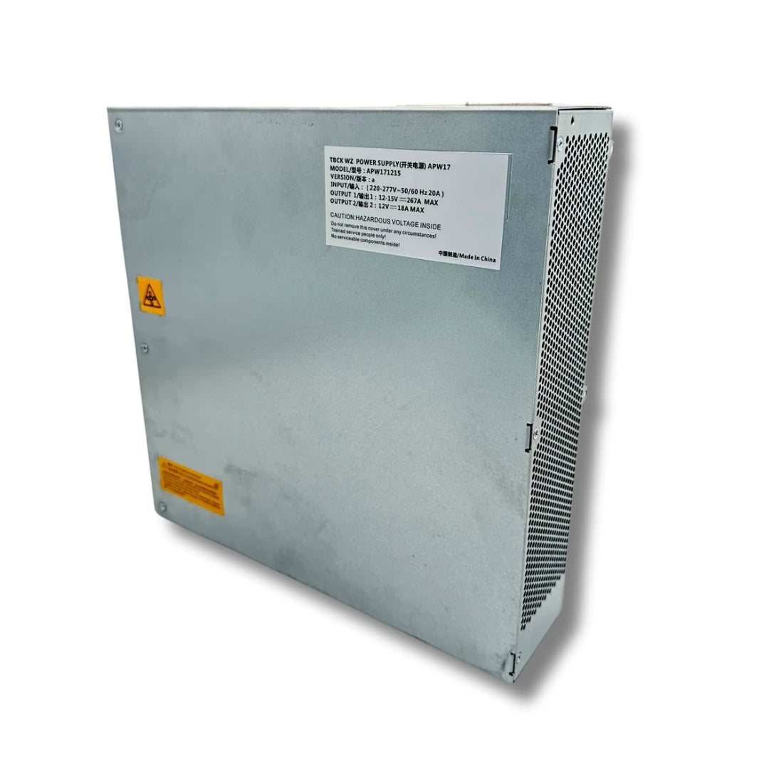
For broader Antminer repair beyond the chips themselves — full hashboards, control boards, PSUs (APW3++ / APW7 / APW8 / APW9 / APW9+ / APW12), fans, cables, and connectors — see our complete Antminer parts catalog or browse the dedicated hashboard repair guides linked throughout this article.
Worldwide shipping from our Shenzhen warehouse via DHL, FedEx, UPS, and sea freight. DDP shipping available for US and EU customers; case-by-case for other lanes — request a quote with your shipping country for confirmation.